
Datasheet


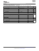


TPS28225
TPS28226
www.ti.com
SLUS710C –MAY 2006–REVISED APRIL 2010
High-Frequency 4-A Sink Synchronous MOSFET Drivers
Check for Samples: TPS28225, TPS28226
1
FEATURES
DESCRIPTION
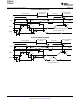
• Drives Two N-Channel MOSFETs with 14-ns
Adaptive Dead Time
The TPS28225 and TPS28226 are high-speed
drivers for N-channel complimentary driven power
• Wide Gate Drive Voltage: 4.5 V Up to 8.8 V
MOSFETs with adaptive dead-time control. These
With Best Efficiency at 7 V to 8 V
drivers are optimized for use in variety of high-current
• Wide Power System Train Input Voltage: 3 V
one and multi-phase dc-to-dc converters. The
Up to 27 V
TPS28225/6 is a solution that provides highly
• Wide Input PWM Signals: 2.0 V up to 13.2-V
efficient, small size low EMI emmissions.
Amplitude
The performance is achieved by up to 8.8-V gate
• Capable Drive MOSFETs with ≥40-A Current
drive voltage, 14-ns adaptive dead-time control, 14-ns
per Phase
propagation delays and high-current 2-A source and
4-A sink drive capability. The 0.4-Ω impedance for
• High Frequency Operation: 14-ns Propagation
the lower gate driver holds the gate of power
Delay and 10-ns Rise/Fall Time Allow F
SW
- 2
MOSFET below its threshold and ensures no
MHz
shoot-through current at high dV/dt phase node
• Capable Propagate <30-ns Input PWM Pulses
transitions. The bootstrap capacitor charged by an
• Low-Side Driver Sink On-Resistance (0.4 Ω)
internal diode allows use of N-channel MOSFETs in
half-bridge configuration.
Prevents dV/dT Related Shoot-Through
Current
The TPS28225/6 features a 3-state PWM input
• 3-State PWM Input for Power Stage Shutdown
compatible with all multi-phase controllers employing
3-state output feature. As long as the input stays
• Space Saving Enable (input) and Power Good
within 3-state window for the 250-ns hold-off time, the
(output) Signals on Same Pin
driver switches both outputs low. This shutdown
• Thermal Shutdown
mode prevents a load from the reversed-
• UVLO Protection
output-voltage.
• Internal Bootstrap Diode
The other features include under voltage lockout,
• Economical SOIC-8 and Thermally Enhanced
thermal shutdown and two-way enable/power good
signal. Systems without 3-state featured controllers
3-mm x 3-mm DFN-8 Packages
can use enable/power good input/output to hold both
• High Performance Replacement for Popular
outputs low during shutting down.
3-State Input Drivers
The TPS28225/6 is offered in an economical SOIC-8
and thermally enhanced low-size Dual Flat No-Lead
APPLICATIONS
(DFN-8) packages. The driver is specified in the
• Multi-Phase DC-to-DC Converters with Analog
extended temperature range of –40°C to 125°C with
or Digital Control
the absolute maximum junction temperature 150°C.
• Desktop and Server VRMs and EVRDs
The TPS28226 operates in the same manner as the
• Portable/Notebook Regulators
TPS28225/6 other than the input under voltage lock
• Synchronous Rectification for Isolated Power
out. Unless otherwise stated all references to the
Supplies
TPS28225 apply to the TPS28226 also.
1
Please be aware that an important notice concerning availability, standard warranty, and use in critical applications of Texas
Instruments semiconductor products and disclaimers thereto appears at the end of this data sheet.
UNLESS OTHERWISE NOTED this document contains
Copyright © 2006–2010, Texas Instruments Incorporated
PRODUCTION DATA information current as of publication date.
Products conform to specifications per the terms of Texas
Instruments standard warranty. Production processing does not
necessarily include testing of all parameters.