
Datasheet


SLVS224B − NOVEMBER 1999 − REVISED AUGUST 2002
11
POST OFFICE BOX 655303 • DALLAS, TEXAS 75265
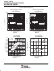
APPLICATION INFORMATION
Great care should be taken when laying out the PC board. The power-processing section is the most critical
and will generate large amounts of EMI if not properly configured. The junction of Q1, Q2, and L1 should be very
tight. The connection from Q1 drain to the positive sides of C5, C10, and C11 and the connection from Q2 source
to the negative sides of C5, C10, and C11 should be as short as possible. The negative terminals of C7 and
C12 should also be connected to Q2 source.
Next, the traces from the MOSFET driver to the power switches should be considered. The BOOTLO signal from
the junction of Q1 and Q2 carries the large gate drive current pulses and should be as heavy as the gate drive
traces. The bypass capacitor (C14) should be tied directly across V
CC
and PGND.
The next most sensitive node is the FB node on the controller (terminal 4 on the TL5001A). This node is very
sensitive to noise pickup and should be isolated from the high-current power stage and be as short as possible.
The ground around the controller and low-level circuitry should be tied to the power ground as the output. If these
three areas are properly laid out, the rest of the circuit should not have other EMI problems and the power supply
will be relatively free of noise.