
Datasheet

SLVS224B − NOVEMBER 1999 − REVISED AUGUST 2002
2
POST OFFICE BOX 655303 • DALLAS, TEXAS 75265
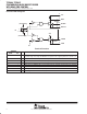
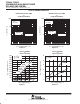
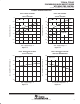
functional block diagram
DT
3
IN
V
CC
LOWDR
BOOTLO
HIGHDR
BOOT
PGND
1
4
8
7
6
5
V
CC
2
(TPS2836 Only)
(TPS2837 Only)
1 MΩ
250 kΩ
250 kΩ
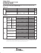
Terminal Functions
TERMINAL
I/O
DESCRIPTION
NAME NO.
I/O
DESCRIPTION
BOOT 8 I Bootstrap terminal. A ceramic capacitor is connected between BOOT and BOOTLO to develop the floating
bootstrap voltage for the high-side MOSFET. The capacitor value is typically between 0.1 µF and 1 µF.
BOOTLO 6 O This terminal connects to the junction of the high-side and low-side MOSFETs.
DT 3 I Dead-time control terminal. Connect DT to the junction of the high-side and low-side MOSFETs
HIGHDR 7 O Output drive for the high-side power MOSFET
IN 1 I Input signal to the MOSFET drivers (noninverting input for the TPS2836; inverting input for the TPS2837).
LOWDR 5 O Output drive for the low-side power MOSFET
PGND 2 Power ground. Connect to the FET power ground.
V
CC
4 I Input supply. Recommended that a 1 µF capacitor be connected from V
CC
to PGND.