
Datasheet

SLVS224B − NOVEMBER 1999 − REVISED AUGUST 2002
3
POST OFFICE BOX 655303 • DALLAS, TEXAS 75265
detailed description
low-side driver
The low-side driver is designed to drive low r
DS(on)
N-channel MOSFETs. The current rating of the driver is 2 A,
source and sink.
high-side driver
The high-side driver is designed to drive low r
DS(on)
N-channel MOSFETs. The current rating of the driver is 2 A,
source and sink. The high-side driver can be configured as a ground-reference driver or a floating bootstrap
driver. The internal bootstrap diode is a Schottky for improved drive efficiency. The maximum voltage that can
be applied between the BOOT terminal and ground is 30 V.
dead-time (DT) control
Dead-time control prevents shoot-through current from flowing through the main power FETs during switching
transitions by controlling the turnon times of the MOSFET drivers. The high-side driver is not allowed to turn
on until the gate drive voltage to the low-side FET is low, and the low-side driver is not allowed to turn on until
the voltage at the junction of the power FETs (Vdrain) is low; the TTL-compatible DT terminal connects to the
junction of the power FETs.
IN
The IN terminal is a TTL-compatible digital terminal that is the input control signal for the drivers. The TPS2836
has a noninverting input; the TPS2837 has an inverting input.
absolute maximum ratings over operating free-air temperature (unless otherwise noted)
†
Supply voltage range, V
CC
(see Note 1) −0.3 V to 16 V. . . . . . . . . . . . . . . . . . . . . . . . . . . . . . . . . . . . . . . . . . . . .
Input voltage range:BOOT to PGND (high-side driver ON) −0.3 V to 30 V. . . . . . . . . . . . . . . . . . . . . . . . . . . . .
BOOTLO to PGND −0.3 V to 16 V. . . . . . . . . . . . . . . . . . . . . . . . . . . . . . . . . . . . . . . . . . . . . .
BOOT to BOOTLO −0.3 V to 16 V. . . . . . . . . . . . . . . . . . . . . . . . . . . . . . . . . . . . . . . . . . . . . .
IN −0.3 V to 16 V. . . . . . . . . . . . . . . . . . . . . . . . . . . . . . . . . . . . . . . . . . . . . . . . . . . . . . . . . . . . .
DT −0.3 V to 30 V. . . . . . . . . . . . . . . . . . . . . . . . . . . . . . . . . . . . . . . . . . . . . . . . . . . . . . . . . . . .
Continuous total power dissipation See Dissipation Rating Table. . . . . . . . . . . . . . . . . . . . . . . . . . . . . . . . . . . . .
Operating virtual junction temperature range, T
J
−40°C to 125°C. . . . . . . . . . . . . . . . . . . . . . . . . . . . . . . . . . . . .
Storage temperature range, T
stg
−65°C to 150°C. . . . . . . . . . . . . . . . . . . . . . . . . . . . . . . . . . . . . . . . . . . . . . . . . . .
Lead temperature soldering 1,6 mm (1/16 inch) from case for 10 seconds 260°C. . . . . . . . . . . . . . . . . . . . . . .
†
Stresses beyond those listed under “absolute maximum ratings” may cause permanent damage to the device. These are stress ratings only, and
functional operation of the device at these or any other conditions beyond those indicated under “recommended operating conditions” is not
implied. Exposure to absolute-maximum-rated conditions for extended periods may affect device reliability.
NOTE 1: Unless otherwise specified, all voltages are with respect to PGND.
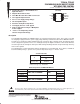
DISSIPATION RATING TABLE
PACKAGE
T
A
≤ 25°C
POWER RATING
DERATING FACTOR
ABOVE T
A
= 25°C
T
A
= 70°C
POWER RATING
T
A
= 85°C
POWER RATING
D 600 mW 6.0 mW/°C 330 mW 240 mW
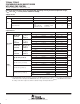
recommended operating conditions
MIN NOM MAX UNIT
Supply voltage, V
CC
4.5 15 V
Input voltage BOOT to PGND 4.5 28 V