
Datasheet

SLVS224B − NOVEMBER 1999 − REVISED AUGUST 2002
4
POST OFFICE BOX 655303 • DALLAS, TEXAS 75265
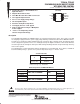
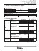
electrical characteristics over recommended operating virtual junction temperature range,
V
CC
= 6.5 V, C
L
= 3.3 nF (unless otherwise noted)
supply current
PARAMETER TEST CONDITIONS MIN TYP MAX UNIT
Supply voltage range 4.5 15 V
Quiescent current V
CC
=15 V, V
(ENABLE)
= LOW 100
A
V
CC
Quiescent current V
CC
=15 V, V
(ENABLE)
= HIGH 300 400
µA
V
CC
Quiescent current
V
CC
=12 V,
f
SWX
= 200 kHz,
C
HIGHDR
= 50 pF,
BOOTLO grounded,
C
LOWDR
= 50 pF,
See Note 2
3 mA
NOTE 2: Ensured by design, not production tested.
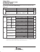
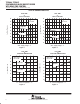
output drivers
PARAMETER TEST CONDITIONS MIN TYP MAX UNIT
High-side sink
Duty cycle < 2%,
V
BOOT
– V
BOOTLO
= 4.5 V, V
HIGHDR
= 4 V 0.7 1.1
High-side sink
(see Note 4)
Duty cycle < 2%,
t
pw
< 100 µs
(see Note 3)
V
BOOT
– V
BOOTLO
= 6.5 V, V
HIGHDR
= 5 V 1.1 1.5
A
(see Note 4)
t
pw
< 100 µs
(see Note 3)
V
BOOT
– V
BOOTLO
= 12 V, V
HIGHDR
= 10.5 V 2 2.4
A
High-side
Duty cycle < 2%,
V
BOOT
– V
BOOTLO
= 4.5 V, V
HIGHDR
= 0.5V 1.2 1.4
High-side
source
(see Note 4)
Duty cycle < 2%,
t
pw
< 100 µs
(see Note 3)
V
BOOT
– V
BOOTLO
= 6.5 V, V
HIGHDR
= 1.5 V 1.3 1.6
A
Peak output-
source
(see Note 4)
t
pw
< 100 µs
(see Note 3)
V
BOOT
– V
BOOTLO
= 12 V, V
HIGHDR
= 1.5 V 2.3 2.7
A
Peak output-
current
Low-side sink
Duty cycle < 2%,
V
CC
= 4.5 V, V
LOWDR
= 4 V 1.3 1.8
current
Low-side sink
(see Note 4)
Duty cycle < 2%,
t
pw
< 100 µs
(see Note 3)
V
CC
= 6.5 V, V
LOWDR
= 5 V 2 2.5
A
(see Note 4)
t
pw
< 100 µs
(see Note 3)
V
CC
= 12 V, V
LOWDR
= 10.5 V 3 3.5
A
Low-side
Duty cycle < 2%,
V
CC
= 4.5 V, V
LOWDR
= 0.5V 1.4 1.7
Low-side
source
(see Note 4)
Duty cycle < 2%,
t
pw
< 100 µs
(see Note 3)
V
CC
= 6.5 V, V
LOWDR
= 1.5 V 2 2.4
A
source
(see Note 4)
t
pw
< 100 µs
(see Note 3)
V
CC
= 12 V, V
LOWDR
= 1.5 V 2.5 3
A
V
BOOT
– V
BOOTLO
= 4.5 V, V
HIGHDR
= 0.5 V 5
High-side sink (see Note 4)
V
BOOT
– V
BOOTLO
= 6.5 V, V
HIGHDR
= 0.5 V 5
Ω
High-side sink (see Note 4)
V
BOOT
– V
BOOTLO
= 12 V, V
HIGHDR
= 0.5 V 5
Ω
V
BOOT
– V
BOOTLO
= 4.5 V, V
HIGHDR
= 4 V 75
High-side source (see Note 4)
V
BOOT
– V
BOOTLO
= 6.5 V, V
HIGHDR
= 6 V 75
Ω
Output
High-side source (see Note 4)
V
BOOT
– V
BOOTLO
= 12 V, V
HIGHDR
=11.5 V 75
Ω
Output
resistance
V
DRV
= 4.5 V, V
LOWDR
= 0.5 V 9
resistance
Low-side sink (see Note 4)
V
DRV
= 6.5 V V
LOWDR
= 0.5 V 7.5
Ω
Low-side sink (see Note 4)
V
DRV
= 12 V, V
LOWDR
= 0.5 V 6
Ω
V
DRV
= 4.5 V, V
LOWDR
= 4 V 75
Low-side source (see Note 4)
V
DRV
= 6.5 V, V
LOWDR
= 6 V 75
Ω
Low-side source (see Note 4)
V
DRV
= 12 V, V
LOWDR
= 11.5 V 75
NOTES: 3. Ensured by design, not production tested.
4. The pullup/pulldown circuits of the drivers are bipolar and MOSFET transistors in parallel. The peak output current rating is the
combined current from the bipolar and MOSFET transistors. The output resistance is the r
DS(on)
of the MOSFET transistor when
the voltage on the driver output is less than the saturation voltage of the bipolar transistor.