
Datasheet


TPS3836E18-Q1 / J25-Q1 / H30-Q1 / L30-Q1 / K33-Q1
TPS3837E18-Q1 / J25-Q1 / L30-Q1 / K33-Q1, TPS3838E18-Q1 / J25-Q1 / L30-Q1 / K33-Q1
NANOPOWER SUPERVISORY CIRCUITS
SGLS141A − DECEMBER 2002 − REVISED JANUARY 2007
1
POST OFFICE BOX 655303 • DALLAS, TEXAS 75265
D Qualified for Automotive Applications
D Customer-Specific Configuration Control
Can Be Supported Along With
Major-Change Approval
D ESD Protection Exceeds 2000 V Per
MIL-STD-883, Method 3015; Exceeds 200 V
Using Machine Model (C = 200 pF, R = 0)
D Supply Current of 220 nA (Typ)
D Precision Supply Voltage Supervision
Range: 1.8 V, 2.5 V, 3.0 V, 3.3 V
D Power-On Reset Generator With Selectable
Delay Time of 10 ms or 200 ms
D Push/Pull RESET Output (TPS3836),
RESET Output (TPS3837), or
Open-Drain RESET
Output (TPS3838)
D Manual Reset
D 5-Pin SOT-23 Package
D Temperature Range: −40°C to 125°C
D Applications Include
− Applications Using Automotive
Low-Power DSPs, Microcontrollers, or
Microprocessors
− Battery-Powered Equipment
− Intelligent Instruments
− Wireless Communication Systems
− Automotive Systems
description
The TPS3836, TPS3837, TPS3838 families of
supervisory circuits provide circuit initialization
and timing supervision, primarily for DSP and
processor-based systems.
During power on, RESET
is asserted when the supply voltage V
DD
becomes higher than 1.1 V. Thereafter, the
supervisory circuit monitors V
DD
and keeps RESET output active as long as V
DD
remains below the threshold
voltage V
IT
. An internal timer delays the return of the output to the inactive state (high) to ensure proper system
reset. The delay time starts after V
DD
has risen above the threshold voltage V
IT
.
When CT is connected to GND a fixed delay time of typical 10 ms is asserted. When connected to V
DD
the delay
time is typically 200 ms.
When the supply voltage drops below the threshold voltage V
IT
, the output becomes active (low) again.
All the devices of this family have a fixed-sense threshold voltage V
IT
set by an internal voltage divider.
The TPS3836 has an active-low push-pull RESET
output. The TPS3837 has active-high push-pull RESET, and
TPS3838 integrates an active-low open-drain RESET
output.
Copyright 2007, Texas Instruments Incorporated
PRODUCTION DATA information is current as of publication date.
Products conform to specifications per the terms of Texas Instruments
standard warranty. Production processing does not necessarily include
testing of all parameters.
Please be aware that an important notice concerning availability, standard warranty, and use in critical applications of
Texas Instruments semiconductor products and disclaimers thereto appears at the end of this data sheet.
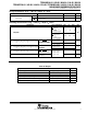
3
2
4
5
(TOP VIEW)
1
CT
GND
MR
V
DD
RESET
TPS3836, TPS3838
DBV PACKAGE
3
2
4
5
(TOP VIEW)
1
CT
GND
MR
V
DD
RESET
TPS3837
DBV PACKAGE