
Incor User's Guide Converter TPS40003

SLUU130A – September 2002 – Revised February 2003
10
TPS40003-Based 5-A Converter in Less Than One Square Inch
5 PowerPAD Packaging
The TPS4000X family is available in the DGQ version of TI’s PowerPAD thermally enhanced package. In the
PowerPAD, a thermally conductive epoxy is utilized to attach the integrated circuit die to the leadframe die
pad, which is exposed on the bottom of the completed package. The leadframe die pad can be soldered to the
PCB using standard solder flow techniques when maximum heat dissipation is required. However, depending
on power dissipation requirements, the PowerPAD may not need to soldered to the PCB.
The PowerPAD package helps to keep the junction temperature rise relatively low even with the power
dissipation inherent in the onboard MOSFET drivers. This power loss is proportional to switching frequency,
drive voltage, and the gate charge needed to enhance the N-channel MOSFETs. Effective heat removal allows
the use of ultra small packaging while maintaining high component reliability.
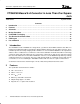
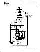
To effectively remove heat from the PowerPAD package, a thermal land should be provided directly
underneath the package whether the package needs to be soldered or not. This thermal land usually has vias
that help to spread heat to internal copper layers and/or the opposite side of the PCB. The vias should not have
thermal reliefs that are often used on ground planes, because this reduces the copper area which transfers heat.
Additionally, the vias should be small enough so that the holes are effectively plugged when plated. This
prevents the solder from wicking away from the connection between the PCB surface and the bottom of the part.
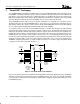
A typical construction utilizes a few vias of 0.013” diameter plated with 1 ounce copper in the land under the
TPS40003. A typical layout pattern is shown in Figure 2, but does not show the copper land which would
encompass the vias above and below the device.
2.92mm
(0.115”)
0.5mm
(0.0197”)
0.28mm
(0.011”)
1.40mm
(0.055”)
Via Dia.
0.33mm
(0.013”)
Miminum
PowerPad ”X”
1.3mm
(0.050”)
Minimum
PowerPad ”Y”
1.7mm
(0.068”)
Figure 3. PowerPAD PCB Layout Guidelines
The Texas Instrument document, PowerPAD Thermally Enhanced Package Application Report (SLMA002)
should be consulted for more information on the PowerPAD package. This report offers in-depth information
on the package, assembly and rework techniques, and illustrative examples of the thermal performance of the
PowerPAD package.