
Datasheet

SLUU189 − July 2004
7
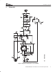
TPS40009-Based 5-A Converter in Less Than One Square Inch
4.4 Output Capacitor Selection
Selection of the output capacitor is based on many application variables, including function, cost, size, and
availability. The minimum allowable output capacitance is determined by the amount of inductor ripple current
and the allowable output ripple in equation (3).
C
OUT(min)
+
I
RIPPLE
8 f V
RIPPLE
+
1.25 A
8 600 kHz 12 mV
+ 22 mF
In this design, C
OUT(min)
is 22 µF with V
RIPPLE
= 12 mV to allow for some margin. However, this only affects the
capacitive component of the ripple voltage. In addition, the voltage component due to the capacitor ESR must
be considered in equation (4).
ESR
Cout
v
V
RIPPLE
I
RIPPLE
+
0.012 V
1.25 A
+ 9.6 mW
For compactness while maintaining transient response capability, two 22-µF ceramic capacitors are fitted in
parallel. The total ESR of these capacitors is below 3 mΩ, and contributes only a few mV to the output voltage
ripple.
4.5 MOSFET Selection
The small physical size of this design requires the use of a single SO-8 package which contains dual N-channel
MOSFETs. MOSFETs with an R
DS(on)
of 18 mΩ are selected to keep the conduction losses to a manageable
amount at full load.
4.6 Short Circuit Protection
The TPS40009 implements short circuit protection by comparing the voltage across the topside MOSFET while
it is on to a voltage dropped from VDD by R
LIM
due to an internal current source of 15 µA inside pin 1. Due to
tolerances in the current source and variations in the power MOSFET on-voltage versus temperature, the short
circuit level can protect against gross overcurrent conditions only, and should be set higher than rated load. In
this particular case, R
LIM
is selected as:
R
LIM
+ R1 +
2.5 I
OUT
0.018 W
15 mA
+ 15 kW
For this design, R
LIM
= 15 kΩ, and the factor of 2.5 in the equation accounts for the variations in component
tolerances over temperature and output current ripple.
(3)
(4)
(5)