
Datasheet

SLUU189 − July 2004
9
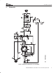
TPS40009-Based 5-A Converter in Less Than One Square Inch
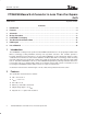
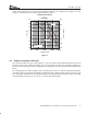
Figure 2 shows the plots for the closed loop gain and phase with V
IN
= 3.3 V and I
OUT
= 4.4 A. At the crossover
frequency of 60 kHz the phase margin is approximately 51 degrees.
100
150
100
50
0
−50
−100
40
30
20
10
0
−10
−20
−30
−40
1000 10000 1000000
Frequency − Hz
100000
Phase
−150
Gain − db
GAIN AND PHASE MARGIN
vs
FREQUENCY
Phase − degrees
I
LOAD
= 4.4 A
V
I
= 3.3 V
Gain
Figure 2.
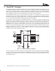
4.8 Snubber Component Selection
The switch node where Q1 and L1 come together is very noisy. An R−C network fitted between this node and
ground can help reduce ringing and voltage overshoot on Q1:B. This ringing noise should be minimized to
prevent it from confusing the control circuitry which is monitoring this node for current limit and Predictive Gate
Drive.
As a starting point, the snubber capacitor, C9, is generally chosen to be 5 to 8 times larger than the parasitic
capacitance at the node, which is primarily C
OS
of Q1:B. Since C
OS
is 440 pF for Q1:B, C9 is chosen to be 3.3 nF.
R3 is empirically determined to be 2.2 Ω, which minimizes the ringing and overshoot at the switch node. With
low input voltages the power loss, 1/2×C×V
2
×f , is relatively small at 24 mW.