TPS40040, TPS40041 www.ti.com SLUS700D – MARCH 2006 – REVISED DECEMBER 2007 LOW PIN COUNT, LOW VIN (2.5 V TO 5.5 V) SYNCHRONOUS BUCK DC-TO-DC CONTROLLER WITH ENABLE FEATURES APPLICATIONS • • • • • • • • • • • 1 23 • • • • • • 2.25-V to 5.5-V Input Output Voltage from 0.6 V to 90% of VIN High-Side Drive for N-Channel FET Supports Pre-Biased Outputs Adaptive Anti-Cross Conduction Gate Drive 1%, 0.
TPS40040, TPS40041 www.ti.com SLUS700D – MARCH 2006 – REVISED DECEMBER 2007 DESCRIPTION (CONT.) One of three short circuit threshold levels may be selected by the addition of an external resistor from the COMP pin to circuit ground. During power on, and before the internal soft start commands the output voltage to rise, the TPS40040/1 enters a calibration cycle, measures the current out of the COMP pin, and selects an internal SCP threshold voltage. At the end of the 1.
TPS40040, TPS40041 www.ti.com SLUS700D – MARCH 2006 – REVISED DECEMBER 2007 ELECTRICAL CHARACTERISTICS TJ = -40 C to 85C VDD = 5 V, (unless otherwise noted) PARAMETER TEST CONDITIONS MIN TYP MAX UNIT Input Supply VDD Input voltage range 2.25 5.5 V IDDsd Shutdown EN = VDD IDDq Quiescent FB = 0.8 V 100 180 µA 1.0 2.0 IDDs Switching current No load at HDRV/LDRV 2.0 UVLOON Minimum turn-on voltage UVLOHYS Hysteresis mA 1.95 2.05 2.
TPS40040, TPS40041 www.ti.com SLUS700D – MARCH 2006 – REVISED DECEMBER 2007 ELECTRICAL CHARACTERISTICS (continued) TJ = -40 C to 85C VDD = 5 V, (unless otherwise noted) PARAMETER TEST CONDITIONS MIN TYP MAX UNIT Soft Start/Enable tCAL (2) Calibration time before softstart begins tSS (2) Soft start time FB rise time from 0 V to 600 mV tREG Time to voltage regulation Sum of tCAL plus tSS VEN Enable threshold EN voltage w.r.t. VDD VENHYS Enable hysteresis 1.0 1.6 2.5 3.0 4.0 6.0 4.
TPS40040, TPS40041 www.ti.com SLUS700D – MARCH 2006 – REVISED DECEMBER 2007 TYPICAL CHARACTERISTICS Quiescent Current (Non-Switching) Shutdown Current 1.100 110 1.000 105 VDD = 5.5 V 100 IDDsd − µA 0.900 IDDq − mA VDD = 2.25 V 0.800 0.700 95 90 85 0.600 80 0.500 VDD = 2.25 V 0.400 −40 −20 VDD = 5.5 V 75 70 0 20 40 60 80 Temperature − C 100 120 −40 −20 0 20 40 60 80 Temperature − C Figure 1. Figure 2. UVLO Threshold EN Threshold −0.8 2.
TPS40040, TPS40041 www.ti.com SLUS700D – MARCH 2006 – REVISED DECEMBER 2007 TYPICAL CHARACTERISTICS (continued) Soft Start Time FB Voltage 4.50 610 VDD = 2.25 V VDD = 3.9 V VDD = 5.5 V 608 VDD = 5 V 4.45 606 604 VFB − mV TSS − ms 4.40 4.35 602 600 598 4.30 596 594 4.25 592 590 4.20 −40 −20 0 20 40 60 80 Temperature − C −40 100 120 −20 0 Figure 7. 20 40 60 80 Temperature − C 100 120 Figure 8. PWM Gain (TPS40040) PWM Gain (TPS40041) 6.1 6.0 VDD = 5 V VDD = 5 V 6.0 5.9 5.
TPS40040, TPS40041 www.ti.com SLUS700D – MARCH 2006 – REVISED DECEMBER 2007 TYPICAL CHARACTERISTICS (continued) Minimum Controllable Pulse Width (TPS40040) Minimum Controllable Pulse Width (TPS40041) 100 130 VDD = 2.25 V 95 VDD = 5.5 V 125 Pulse Width − ns Pulse Width − ns 90 120 115 110 85 80 75 105 70 100 65 VDD = 2.25 V 95 −40 −20 0 20 40 60 80 Temperature − C 60 −40 100 120 −20 0 Figure 13. 20 40 60 80 Temperature − C 100 120 Figure 14.
TPS40040, TPS40041 www.ti.com SLUS700D – MARCH 2006 – REVISED DECEMBER 2007 DEVICE INFORMATION TERMINAL CONFIGURATION The package is an 8-pin SON (DRB) package. Note: The thermal pad is an electrical ground connection. TPS40040/1 1 EN HDRV 8 2 FB SW 7 3 COMP BOOT 6 4 VDD LDRV 5 GND Figure 17. DRB Package Terminal Configuration (Top View) Table 1. TERMINAL FUNCTIONS TERMINAL NAME BOOT COMP NO.
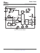
TPS40040, TPS40041 www.ti.com SLUS700D – MARCH 2006 – REVISED DECEMBER 2007 Block Diagram VDD VDD 4 VDD/2 UVLO SW SDN 100K 2V EN EN 1 100ns DELAY FAULT LOGIC ILIM SET CURRENT LIMIT COMP Vdd−1.2v VDD SDN CLOCK 0.6 V VREF Soft Start FB 2 COMP 3 LDRV PWM COMP + + − PWM PWM LOGIC RAMP VDD OSCILLATOR 0.
TPS40040, TPS40041 www.ti.com SLUS700D – MARCH 2006 – REVISED DECEMBER 2007 APPLICATION INFORMATION Functional Description The TPS40040 (300 kHz) and TPS40041 (600 kHz) are fixed-frequency voltage-mode synchronous buck controllers. In operation, the synchronous rectifier (SR) is allowed to conduct current in both directions, allowing a converter to operate in continuous mode, even under no load conditions, simplifying feedback loop compensation requirements.
TPS40040, TPS40041 www.ti.com SLUS700D – MARCH 2006 – REVISED DECEMBER 2007 Enable and Start-Up Sequence The EN pin of the TPS40040/1s internally pulled to VDD. When power is applied to VDD, the EN pin is allowed to float high, and the TPS40040/1 remains OFF. Only when the EN pin is externally pulled below the threshold voltage of VDD - 1.2 V is the TPS40040/1 allowed to start. When enabled, the TPS40040/1 enters a calibration cycle where the short circuit current threshold is determined.
TPS40040, TPS40041 www.ti.com SLUS700D – MARCH 2006 – REVISED DECEMBER 2007 Pre-Bias Startup The TPS40040/1 supports pre-biased output voltage applications. In cases where the output voltage is held up by external means while the TPS40040/1 is off, full synchronous rectification is disabled during the initial phase of soft starting the output voltage.
TPS40040, TPS40041 www.ti.com SLUS700D – MARCH 2006 – REVISED DECEMBER 2007 Output Short Circuit Protection To minimize circuit losses, the TPS40040/1 uses the RDS(on) of the upper MOSFET switch as the current sensing element. The current limit comparator, initially blanked during the first portion of each switching cycle, senses the voltage across the high-side MOSFET when it is fully ON. This voltage is compared to an internally selected short circuit current (SCC) limit threshold voltage.
TPS40040, TPS40041 www.ti.com SLUS700D – MARCH 2006 – REVISED DECEMBER 2007 Gate Drive Resistors The TPS40040/41’s adaptive gate delay circuitry monitors the HDRV-to-SW and LDRV-to-GND voltages to determine the state of the external MOSFET switches. Any voltage drop across an external series gate drive resistor is sensed as reduced gate voltage during turn-off and may interfere with the MOSFET timing.
TPS40040, TPS40041 www.ti.com SLUS700D – MARCH 2006 – REVISED DECEMBER 2007 Bootstrap for N-Channel MOSFET Drive The PWM duty cycle is limited to a maximum of 95%, allowing the bootstrap capacitor to charge during every cycle. During each PWM OFF period, the voltage on VDD charges the bootstrap capacitor. When the PWM switch is next commanded to turn ON, the voltage used to drive the MOSFET is derived from the voltage on this capacitor.
TPS40040, TPS40041 www.ti.com SLUS700D – MARCH 2006 – REVISED DECEMBER 2007 VDD Filter Resistor To further limit the noise on VDD, a small 1-Ω to 2-Ω resistor may be placed between the input voltage and the VDD pin to create a small filter to VDD. The resistor should connect near the drain of the upper switch MOSFET to prevent trace IR drops from increasing the sensed voltage drop. The resistor itself should be placed close to Pin 4.
TPS40040, TPS40041 www.ti.com SLUS700D – MARCH 2006 – REVISED DECEMBER 2007 PCB Layout Guidelines A synchronous BUCK power stage has two primary current loops, the input current loop that carries high ac discontinuous current and an output current loop that carries high dc continuous current. The output current loop carries low ac inductor ripple current.
TPS40040, TPS40041 www.ti.com SLUS700D – MARCH 2006 – REVISED DECEMBER 2007 Device to Power Stage Interface The TPS40040/1 uses a very fast break-before-make anti-cross conduction circuit to minimize power loss. Adding external impedance in series with the gates of the switching MOSFETs adversely affects the converter’s operation and must be avoided.
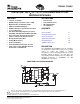
TPS40040, TPS40041 www.ti.com SLUS700D – MARCH 2006 – REVISED DECEMBER 2007 DESIGN EXAMPLES Example 1. A 5-V to 1.8-V DC-to-DC Converter Using a TPS40041 The following example illustrates the design process and component selection for a 5-V to 1.8-V point-of-load synchronous buck converter. The design goal parameters are given in the table below. A list of symbol definitions is found at the end of this section.
TPS40040, TPS40041 www.ti.com SLUS700D – MARCH 2006 – REVISED DECEMBER 2007 Inductor Selection The inductor is typically sized for 30% peak-to-peak ripple current (IRIPPLE) Given this target ripple current, the required inductor size is calculated by: V IN(max) * V OUT VOUT 1 L+ 0.3 I OUT V IN(max) F SW (4) Solving with VIN(max) = 5.5 V, an inductor value of 1.12 µH is obtained. A standard value of 1.0 µH is selected, resulting in 2-A peak-peak ripple.
TPS40040, TPS40041 www.ti.com SLUS700D – MARCH 2006 – REVISED DECEMBER 2007 Peak Current Rating of Inductor With output capacitance known, it is now possible to calculate the charging current during start-up and determine the minimum saturation current rating for the inductor. The start-up charging current is approximated by: V COUT I CHARGE + OUT T SS (9) Using the TPS40041’s fixed 4.5-ms soft-start time, COUT = 200 µF and VOUT = 1.8 V, ICHARGE is found to be 80 mA.
TPS40040, TPS40041 www.ti.com SLUS700D – MARCH 2006 – REVISED DECEMBER 2007 MOSFET Switch Selection (Q1 & Q2) The switching losses for the upper switch MOSFET are estimated by: P G1SW + 1 2 V IN I OUT ǒT RISE ) T FALLǓ F SW + V IN I OUT Q GS2_Q1 ) Q GD_Q1 VDD*V TH R DRIVE F SW (14) For this design, switching losses are higher at low input voltage due to the lower gate drive current.
TPS40040, TPS40041 www.ti.com SLUS700D – MARCH 2006 – REVISED DECEMBER 2007 Bootstrap Capacitor (C7) To ensure proper charging of the upper switch MOSFET gate, limit the ripple voltage on the bootstrap capacitor to < 5% of the minimum gate drive voltage of 3.0 V. 20 Q GS_Q1 C BOOST + V IN(min) (19) Based on the IRF7910 MOSFET with a maximum total gate charge of 26 nC, calculate a minimum of 116 nF of capacitance. The next higher standard value of 220 nF is selected. VDD Bypass Capacitor (C6) Select a 1.
TPS40040, TPS40041 www.ti.com SLUS700D – MARCH 2006 – REVISED DECEMBER 2007 Feedback Loop Design To design feedback circuit, a small signal average modeling technique is employed. Further information on this technique may be found in the references. Modeling the Power Stage The peak-to-peak ramp voltage given in the Electrical Specification table allows the modulator gain to be calculated as: V IN A MOD + VRAMP(p*p) (22) For this design, a modulator gain of 7.3 (17.3 dB) is calculated.
TPS40040, TPS40041 www.ti.com SLUS700D – MARCH 2006 – REVISED DECEMBER 2007 Error Amplifier Pole-Zero Selection Place two zeros at 80% and 125% of the resonance frequency to keep the actual resonance frequency between the two zeros over the L and C tolerance. For FRES = 11.3 kHz, FZ1 = 9.0 kHz and FZ2 = 14 kHz. Selecting the cross-over frequency (FCO) of the control loop between 3 times the LC filter resonance and 1/5th the switching frequency.
TPS40040, TPS40041 www.ti.com SLUS700D – MARCH 2006 – REVISED DECEMBER 2007 Feedback Components (R3, R6, C3, C4, C5) Approximate C5 with the formula: 1 C5 + 2 p R8 F Z2 (28) C5 = 560 pF (closest standard capacitor value to calculated 568 pF) and approximate R6 with the formula: 1 R6 + 2 p C5 F P1 (29) R6 = 4.75 kΩ (closest standard resistor value to calculated 4.74 kΩ) Calculate R3 by the formula: A MID(band) (R6 R8) R3 + R6 ) R8 (30) With AMID_BAND = 3.84, R6 = 4.75 kΩ and R8 = 20 kΩ, R3 = 14.
TPS40040, TPS40041 www.ti.com SLUS700D – MARCH 2006 – REVISED DECEMBER 2007 100% η − Efficiency − % 90% 80% 4.5 5 5.5 70% 60% 50% 0 1 2 4 3 6 5 7 IOUT − Load Current − A Figure 26. Typical Efficency for 5-V to 1.8-V at 6-A Converter Using TPS40041 1.818 VOUT − Output Voltage − V 1.816 1.814 4.5 1.812 5 5.5 1.810 1.808 1.806 1.804 1.802 1.800 0 1 2 3 4 5 6 7 IOUT − Load Current − A Figure 27. Typical Line/Load Regulation for 5-V to 1.
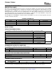
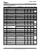
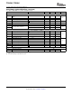
TPS40040, TPS40041 www.ti.com SLUS700D – MARCH 2006 – REVISED DECEMBER 2007 List of Materials REF QTY C1 1 Capacitor, ceramic, 6.3 V, X5R, 20%, 100 µF, 1210 TDK C325X5R0J107M C2 1 Capacitor, ceramic, 6.
TPS40040, TPS40041 www.ti.
TPS40040, TPS40041 www.ti.com SLUS700D – MARCH 2006 – REVISED DECEMBER 2007 Example 2. A 2.5-V to 1.2-V DC-to-DC Converter Using a TPS40041 This example illustrates a 2.5-V to 1.2-V at 3-A synchronous buck application using the TPS40041. A diode has been added to increase the bootstrap capacitor charging current at low input voltage. The highest current limit threshold has been selected due to the increased RDS(on) at low input voltages. Figure 28. Schematic for 2.5-V to 1.
TPS40040, TPS40041 www.ti.com SLUS700D – MARCH 2006 – REVISED DECEMBER 2007 Example 3. A 3.3-V to 1.2-V DC-to-DC Converter Using a TPS40040 This example illustrates a 3.3-V to 1.2-V at 10-A synchronous BUCK application using the TPS40040 switching at 300 kHz. Separate SO-8 MOSFETs have been chosen to support the higher currents in this application and a resistor has been added in series with the BOOT pin to slow the rising edge of the switch node and reduce EMI on the input of the converter. Figure 31.
TPS40040, TPS40041 www.ti.com SLUS700D – MARCH 2006 – REVISED DECEMBER 2007 ADDITIONAL REFERENCES Related Parts The following parts have characteristics similar to the TPS40040/1 and may be of interest.
PACKAGE MATERIALS INFORMATION www.ti.com 9-Apr-2014 TAPE AND REEL INFORMATION *All dimensions are nominal Device Package Package Pins Type Drawing SPQ Reel Reel A0 Diameter Width (mm) (mm) W1 (mm) B0 (mm) K0 (mm) P1 (mm) W Pin1 (mm) Quadrant TPS40040DRBR SON DRB 8 3000 330.0 12.4 3.3 3.3 1.1 8.0 12.0 Q2 TPS40040DRBR SON DRB 8 3000 330.0 12.4 3.3 3.3 1.1 8.0 12.0 Q2 TPS40040DRBT SON DRB 8 250 180.0 12.4 3.3 3.3 1.1 8.0 12.
PACKAGE MATERIALS INFORMATION www.ti.com 9-Apr-2014 *All dimensions are nominal Device Package Type Package Drawing Pins SPQ Length (mm) Width (mm) Height (mm) TPS40040DRBR SON DRB 8 3000 367.0 367.0 35.0 TPS40040DRBR SON DRB 8 3000 367.0 367.0 35.0 TPS40040DRBT SON DRB 8 250 210.0 185.0 35.0 TPS40040DRBT SON DRB 8 250 210.0 185.0 35.0 TPS40041DRBR SON DRB 8 3000 370.0 355.0 55.0 TPS40041DRBT SON DRB 8 250 220.0 205.0 50.
IMPORTANT NOTICE Texas Instruments Incorporated and its subsidiaries (TI) reserve the right to make corrections, enhancements, improvements and other changes to its semiconductor products and services per JESD46, latest issue, and to discontinue any product or service per JESD48, latest issue. Buyers should obtain the latest relevant information before placing orders and should verify that such information is current and complete.