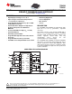
TPS40060 TPS40061 8 www.ti.com SLUS543F – DECEMBER 2002 – REVISED JUNE 2013 WIDE-INPUT SYNCHRONOUS BUCK CONTROLLER Check for Samples: TPS40060, TPS40061 FEATURES APPLICATIONS • • • • • • • • 1 2 • • • • • • • Operating Input Voltage 10 V to 55 V Input Voltage Feed-Forward Compensation < 1% Internal 0.
TPS40060 TPS40061 SLUS543F – DECEMBER 2002 – REVISED JUNE 2013 www.ti.com This integrated circuit can be damaged by ESD. Texas Instruments recommends that all integrated circuits be handled with appropriate precautions. Failure to observe proper handling and installation procedures can cause damage. ESD damage can range from subtle performance degradation to complete device failure.
TPS40060 TPS40061 www.ti.com SLUS543F – DECEMBER 2002 – REVISED JUNE 2013 ELECTRICAL CHARACTERISTICS TA = –40°C to 85°C, VIN = 24 Vdc, RT = 165 kΩ, IKFF = 113 µA, fSW = 300 kHz, all parameters at zero power dissipation (unless otherwise noted) PARAMETER TEST CONDITIONS MIN TYP MAX UNIT INPUT SUPPLY VIN Input voltage range, VIN 10 55 V 1.5 2.5 mA 4.5 5.0 5.
TPS40060 TPS40061 SLUS543F – DECEMBER 2002 – REVISED JUNE 2013 www.ti.com ELECTRICAL CHARACTERISTICS (continued) TA = –40°C to 85°C, VIN = 24 Vdc, RT = 165 kΩ, IKFF = 113 µA, fSW = 300 kHz, all parameters at zero power dissipation (unless otherwise noted) PARAMETER TEST CONDITIONS MIN TYP MAX TA = 25°C 8.8 10.0 11.4 0°C ≤ TA ≤ 85°C 8.3 11.9 -40°C ≤ TA ≤ 0°C 7.5 11.5 UNIT CURRENT LIMIT ISINK Current limit sink current VILIM = 23.7 V, VSW = (VILIM – 0.
TPS40060 TPS40061 www.ti.com SLUS543F – DECEMBER 2002 – REVISED JUNE 2013 Terminal Functions TERMINAL NAME NO. I/O DESCRIPTION BP5 3 O 5-V reference. This pin should be bypassed to ground with a 0.1-µF ceramic capacitor. This pin may be used with an external DC load of 1 mA or less. BP10 11 O 10-V reference used for gate drive of the N-channel synchronous rectifier. This pin should be bypassed by a 1-µF ceramic capacitor. This pin may be used with an external DC load of 1 mA or less.
TPS40060 TPS40061 SLUS543F – DECEMBER 2002 – REVISED JUNE 2013 www.ti.com SIMPLIFIED BLOCK DIAGRAM ILIM 16 VIN 15 11 BP10 13 BPN10 14 HDRV 12 SW BP10 + CLK RT 2 SYNC 4 CLK 7 Clock Oscillator 7 10−V Regulator VIN 7 1V5REF 7 HDRV 7 Ramp Generator KFF Reference Voltages 1 07VREF 7 1V5REF 7 3V5REF 7 BP5 HDRV 7 7 CL 3−bit up/down Fault Counter P-Channel Driver 7 7 7 7 BPN10 Restart Fault BP5 COMP 3 BP5 7 7 Fault 8 07VREF 7 VFB 7 7 + 0.
TPS40060 TPS40061 www.ti.com SLUS543F – DECEMBER 2002 – REVISED JUNE 2013 APPLICATION INFORMATION The TPS40060/61 family of parts allows the user to optimize the PWM controller to the specific application. The TPS40061 is the controller of choice for synchronous buck designs which will include most applications. It has two quadrant operation and will source or sink output current. This provides the best transient response.
TPS40060 TPS40061 SLUS543F – DECEMBER 2002 – REVISED JUNE 2013 www.ti.com The PWM ramp must be faster than the master clock frequency or the PWM is prevented from starting. The PWM ramp time is programmed via a single resistor (RKFF) pulled up to VIN. RKFF is related to RT, and the minimum input voltage, VIN(min) through the following: ǒ Ǔ ǒ65.27 R KFF + VIN (min) * 3.
TPS40060 TPS40061 www.ti.com SLUS543F – DECEMBER 2002 – REVISED JUNE 2013 where: • • VIN is the desired start-up (UVLO) input voltage RT is the timing resistor in kΩ (3) The variable UVLO function utilizes a 3-bit full adder to prevent spurious shut-downs or turn-ons due to spikes or fast line transients.
TPS40060 TPS40061 SLUS543F – DECEMBER 2002 – REVISED JUNE 2013 www.ti.com The impedance of the input voltage can cause the input voltage, at the TPS4006x, to sag when the converter starts to operate and draw current from the input source. Therefore, there is voltage hysteresis that prevents nuisance shutdowns at the UVLO point. With RT chosen to select the operating frequency and RKFF chosen to select the start-up voltage, the amount of hysteresis voltage is shown in Figure 5.
TPS40060 TPS40061 www.ti.com SLUS543F – DECEMBER 2002 – REVISED JUNE 2013 PROGRAMMING CURRENT LIMIT This device uses a two-tier approach for overcurrent protection. The first tier is a pulse-by-pulse protection scheme. Current limit is implemented on the high-side MOSFET by sensing the voltage drop across the MOSFET when the gate is driven low. The MOSFET voltage is compared to the voltage dropped across a resistor connected from VIN pin to the ILIM pin when driven by a constant current sink.
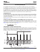
TPS40060 TPS40061 SLUS543F – DECEMBER 2002 – REVISED JUNE 2013 www.ti.com HDRV CLOCK tBLANKING VILIM VVIN-VSW SS 7 CURRENT LIMIT TRIPS (HDRV CYCLE TERMINATED BY CURRENT LIMIT TRIP) 7 SOFT-START CYCLES UDG-02136 Figure 6. Typical Current Limit Protection Waveforms INTERNAL REGULATOR OUTPUT VOLTAGE vs INPUT VOLTAGE 12 BP10 VBPx - Output Voltage - V 10 8 BP5 6 BPN10 4 2 0 2 4 6 8 10 12 VIN - Input Voltage - V Figure 7.
TPS40060 TPS40061 www.ti.com SLUS543F – DECEMBER 2002 – REVISED JUNE 2013 C BPN10 + Qg DV (F) (8) The 10-V reference pin, BP10V needs to provide energy for the synchronous MOSFET gate drive via the BP10V capacitor. Neglecting any efficiency penalty, the BP10V capacitance is described in Equation 9. Q gSR C BP10V + (F) (9) DV SYNCHRONIZING TO AN EXTERNAL SUPPLY The TPS4006x can be synchronized to an external clock through the SYNC pin. The SW node rises on the falling edge of the SYNC signal.
TPS40060 TPS40061 SLUS543F – DECEMBER 2002 – REVISED JUNE 2013 www.ti.com CALCULATING THE OUTPUT CAPACITANCE The output capacitance depends on the output ripple voltage requirement, output ripple current, as well as any output voltage deviation requirement during a load transient. The output ripple voltage is a function of both the output capacitance and capacitor ESR. The worst case output ripple is described in Equation 13.
TPS40060 TPS40061 www.ti.com SLUS543F – DECEMBER 2002 – REVISED JUNE 2013 Duty cycle, D, varies from 0 to 1 as the control voltage, VC, varies from the minimum ramp voltage to the maximum ramp voltage, VS. Also, for a synchronous buck converter, D = VO / VIN. To get the control voltage to output voltage modulator gain in terms of the input voltage and ramp voltage, V V VO V D + O + C or + IN VS V IN VS VC (19) With the voltage feedforward function, the ramp slope is proportional to the input voltage.
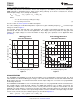
TPS40060 TPS40061 SLUS543F – DECEMBER 2002 – REVISED JUNE 2013 www.ti.com MODULATOR GAIN vs SWITCHING FREQUENCY PWM MODULATOR RELATIONSHIPS ESR Zero, + 1 Modulator Gain - dB AMOD = VIN(min) / VRAMP VS VC Resultant, - 1 D = VC / VS LC Filter, - 2 100 1k 10 k fSW - Switching Frequency - Hz Figure 8. Figure 9. C2 (optional) C1 R3 −1 +1 0 dB R2 −1 GAIN −90° C3 100 k VFB R1 180° 7 8 VOUT COMP + RBIAS VREF PHASE −270° UDG−02189 Figure 10.
TPS40060 TPS40061 www.ti.com SLUS543F – DECEMBER 2002 – REVISED JUNE 2013 The modulator gain as a function of frequency at fC, is described in Equation 27. AMOD(f) + AMOD ǒ Ǔ f LC fC 2 and G+ 1 AMOD(f) (27) Care must be taken not to load down the output of the error amplifier with the feedback resistor, R2, that is too small. The error amplifier has a finite output source and sink current which must be considered when sizing R2.
TPS40060 TPS40061 SLUS543F – DECEMBER 2002 – REVISED JUNE 2013 www.ti.com ID2 IO ID1 d } ∆I 1-d BODY DIODE CONDUCTION BODY DIODE CONDUCTION SW 0 SYNCHRONOUS RECTIFIER ON ANTI-CROSS CONDUCTION HIGH SIDE ON UDG-02179 Figure 12. Inductor Current and SW Node Waveforms The maximum allowable power dissipation in the MOSFET is determined by the following equation. PT + ǒTJ * TAǓ q JA (W) (32) where: P T + PCOND ) PSW(fsw) (W) (33) and ΘJA is the package thermal impedance.
TPS40060 TPS40061 www.ti.com SLUS543F – DECEMBER 2002 – REVISED JUNE 2013 TPS40060/TPS40061 POWER DISSIPATION The power dissipation in the TPS40060 and TPS40061 is largely dependent on the MOSFET driver currents and the input voltage. The driver current is proportional to the total gate charge, Qg, of the external MOSFETs. Driver power (neglecting external gate resistance, (refer to the second reference in the REFERENCES section) can be calculated from Equation 38.
TPS40060 TPS40061 SLUS543F – DECEMBER 2002 – REVISED JUNE 2013 www.ti.com LAYOUT CONSIDERATIONS THE PowerPAD™ PACKAGE The PowerPAD package provides low thermal impedance for heat removal from the device. The PowerPAD derives its name and low thermal impedance from the large bonding pad on the bottom of the device. For maximum thermal performance, the circuit board must have an area of solder-tinned-copper underneath the package. The dimensions of this area depends on the size of the PowerPAD package.
TPS40060 TPS40061 www.ti.com SLUS543F – DECEMBER 2002 – REVISED JUNE 2013 Component placement should ensure that bypass capacitors (BP10, BP5, and BPN10) are located as close as possible to their respective power and ground pins. Also, sensitive circuits such as FB, RT and ILIM should not be located near high dv/dt nodes such as HDRV, LDRV, BPN10, and the switch node (SW).
TPS40060 TPS40061 SLUS543F – DECEMBER 2002 – REVISED JUNE 2013 www.ti.com DESIGN EXAMPLE • • • • • • • Input voltage: 18 VDC to 55 VDC Output voltage: 3.3 V ±2% Output current: 5 A (maximum, steady-state), 7 A (surge, 10-ms duration, 10% duty cycle maximum) Output ripple: 33 mVP-P at 5 A Output load response: 0.3 V => 10% to 90% step load change Operating temperature: –40°C to 85°C fSW = 130 kHz 1. Calculate maximum and minimum duty cycles d MIN + V O(min) VIN(max) + 0.
TPS40060 TPS40061 www.ti.com SLUS543F – DECEMBER 2002 – REVISED JUNE 2013 T J + ǒPCOND ) PSWǓ q JA ) T A + (0.324 ) 0.715) 40 ) 85 + 127 C O (50) 5. Calculate synchronous rectifier losses The synchronous rectifier MOSFET has two loss components, conduction, and diode reverse recovery losses. The conduction losses are due to IRMS losses as well as body diode conduction losses during the dead time associated with the anti-cross conduction delay.
TPS40060 TPS40061 SLUS543F – DECEMBER 2002 – REVISED JUNE 2013 www.ti.com 9. Calculating the Output Capacitance (CO) In this example. the output capacitance is determined by the load response requirement of ΔV = 0.3 V for a 1 A to 5 A step load. CO can be calculated using Equation 18. 10 mH ǒ5 2 * 1 2Ǔ CO + + 127 mF ǒ3.3 2 * 3.0 2Ǔ (60) Using Equation 13 calculate the ESR required to meet the output ripple requirements. ǒ 33 mV + 2.0 ESR ) 8 1 127 mF 130 kHz Ǔ (61) ESR = 8.
TPS40060 TPS40061 www.ti.com SLUS543F – DECEMBER 2002 – REVISED JUNE 2013 The amplifier gain at the crossover frequency of 10 kHz is determined by the reciprocal of the modulator gain AMOD at the crossover frequency from Equation 27. 2 2 æf ö æ 3.7 kHz ö AMOD(f ) = AMOD ´ ç LC ÷ = 9 ´ ç ÷ = 1.23 è 10 kHz ø è fC ø (70) And also from Equation 27. 1 1 G= = = 0.81 AMOD(f ) 1.23 (71) Choose R1 = 100 kΩ The poles and zeros for a Type III network are described in Equation 25 and Equation 26.
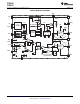
TPS40060 TPS40061 SLUS543F – DECEMBER 2002 – REVISED JUNE 2013 RKFF 301 kΩ + www.ti.com RILIM 174 kΩ 1 TPS40060PWP KFF ILIM 16 2 RT VIN 15 3 BP5 HDRV 14 RT 412 kΩ VIN 2Ω Si9407 0.1 µF − 4 SYNC BPN10 13 0.1 µF RSW 10 Ω CSS 5 SGND SW 12 6 SS/SD BP10 11 7 VFB LDRV 10 8 COMP PGND 9 30BQ060 10 µH 1.0 µF Si4470 3300 pF R3 4.64 kΩ R1 100kΩ + CO 180 µF C1 3900 pF R2 10 kΩ VOUT C3 470 pF − PGND RBIAS 26.7 kΩ C2 220 pF UDG−02161 Figure 14. Design Example, 48 V to 3.
TPS40060 TPS40061 www.ti.com SLUS543F – DECEMBER 2002 – REVISED JUNE 2013 REVISION HISTORY Changes from Revision E (June 2006) to Revision F Page • Changed reference to Figure 13, PowerPad Dimensions, to Figure 14, Design Example, 48 V to 3.3 V at 5 A dc-todc Converter ......................................................................................................................................................................... 7 • Changed both (CSS – 0.85 V) voltages to (VCSS – 0.
TPS40060 TPS40061 SLUS543F – DECEMBER 2002 – REVISED JUNE 2013 www.ti.com 21.5 to 10 kΩ; Equation 76, 21.5 to 10 kΩ, 2000 to 4301 pF, 1800 to 3900 pF ................................................................ 25 • Changed Design Example graphic to include new values from equation: 133 to 301 kΩ, 1800 to 3900 pF, 21.5 to 10 kΩ, 100 to 220 pF. Si9470 to Si9407 .................................................................................................................................
PACKAGE OPTION ADDENDUM www.ti.
PACKAGE OPTION ADDENDUM www.ti.com 11-Apr-2013 (4) Multiple Top-Side Markings will be inside parentheses. Only one Top-Side Marking contained in parentheses and separated by a "~" will appear on a device. If a line is indented then it is a continuation of the previous line and the two combined represent the entire Top-Side Marking for that device. Important Information and Disclaimer:The information provided on this page represents TI's knowledge and belief as of the date that it is provided.
PACKAGE MATERIALS INFORMATION www.ti.com 14-Jul-2012 TAPE AND REEL INFORMATION *All dimensions are nominal Device Package Package Pins Type Drawing SPQ Reel Reel A0 Diameter Width (mm) (mm) W1 (mm) TPS40060PWPR HTSSOP PWP 16 2000 330.0 12.4 TPS40061PWPR HTSSOP PWP 16 2000 330.0 12.4 Pack Materials-Page 1 B0 (mm) K0 (mm) P1 (mm) W Pin1 (mm) Quadrant 6.9 5.6 1.6 8.0 12.0 Q1 6.9 5.6 1.6 8.0 12.
PACKAGE MATERIALS INFORMATION www.ti.com 14-Jul-2012 *All dimensions are nominal Device Package Type Package Drawing Pins SPQ Length (mm) Width (mm) Height (mm) TPS40060PWPR HTSSOP PWP 16 2000 367.0 367.0 35.0 TPS40061PWPR HTSSOP PWP 16 2000 367.0 367.0 35.
IMPORTANT NOTICE Texas Instruments Incorporated and its subsidiaries (TI) reserve the right to make corrections, enhancements, improvements and other changes to its semiconductor products and services per JESD46, latest issue, and to discontinue any product or service per JESD48, latest issue. Buyers should obtain the latest relevant information before placing orders and should verify that such information is current and complete.