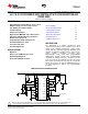
TPS40195 www.ti.com SLUS720E – FEBRUARY 2007 – REVISED JULY 2012 4.5-V TO 20-V SYNCHRONOUS BUCK CONTROLLER WITH SYNCHRONIZATION AND POWER GOOD Check for Samples: TPS40195 FEATURES CONTENTS 1 • • • • • • • • • • • Input Operating Voltage Range: 4.5 V to 20 V Output Voltage as Low as 0.591 V ±0.
TPS40195 SLUS720E – FEBRUARY 2007 – REVISED JULY 2012 www.ti.com These devices have limited built-in ESD protection. The leads should be shorted together or the device placed in conductive foam during storage or handling to prevent electrostatic damage to the MOS gates. DESCRIPTION (CONTINUED) The threshold is set with a single external resistor connected from ILIM to GND.
TPS40195 www.ti.com SLUS720E – FEBRUARY 2007 – REVISED JULY 2012 PACKAGE DISSIPATION RATINGS RθJA High-K Board (1) (°C/W) Power Rating (W) TA = 25°C Power Rating (W) TA = 85°C 0 (Natural Convection) 110 0.90 0.36 0 (Natural Convection) 49.2 2.0 0.81 200 41.2 2.4 0.97 400 37.7 2.6 1.0 PACKAGE AIRFLOW (LFM) PW RGY (1) Ratings based on JEDEC High Thermal Conductivity (High K) Board. For more information on the test method, see TI Technical Brief SZZA017.
TPS40195 SLUS720E – FEBRUARY 2007 – REVISED JULY 2012 www.ti.com ELECTRICAL CHARACTERISTICS (continued) TJ = –40°C to 85°C, VVDD= 12 Vdc, all parameters at zero power dissipation (unless otherwise noted) PARAMETER TEST CONDITIONS MIN TYP MAX UNIT PWM (2) DMAX Maximum duty cycle tON(min) Minimum controlled pulse (2) tDEAD 85% Output driver dead time 130 HDRV off to LDRV on 50 LDRV off to HDRV on 25 VSS_SEL = 0 V, fSW = 250 kHz 4.8 VSS_SEL = 0 V, fSW = 500 kHz 2.
TPS40195 www.ti.
TPS40195 SLUS720E – FEBRUARY 2007 – REVISED JULY 2012 www.ti.com TYPICAL CHARACTERISTICS INPUT CURRENT vs JUNCTION TEMPERATURE OPERATING CURRENT IN SHUTDOWN vs JUNCTION TEMPERATURE 400 3.0 IDD - Input Current - mA 2.5 2.0 VVDD = 12 V 1.5 1.0 0.
TPS40195 www.ti.com SLUS720E – FEBRUARY 2007 – REVISED JULY 2012 TYPICAL CHARACTERISTICS (continued) RELATIVE OVERCURRENT TRIP POINT vs FREEWHEEL TIME EN THRESHOLD VOLTAGES vs JUNCTION TEMPERATURE 5.0 3.0 VIN, VIL - Enable Thresholds Voltage - V IOC - Relative Overcurrent Trip Point - A 4.5 4.0 3.5 3.0 2.5 2.0 1.5 1.0 0.5 0 0.4 0.6 0.8 1.0 1.2 1-D - Freewheel Time - ms 1.4 2.0 1.5 1.0 Off 0.5 On Off 5 20 35 50 65 80 95 110 125 TJ - Junction Temperature - °C Figure 5. Figure 6.
TPS40195 SLUS720E – FEBRUARY 2007 – REVISED JULY 2012 www.ti.com TYPICAL CHARACTERISTICS (continued) BP DROPOUT VOLTAGE vs JUNCTION TEMPERATURE UNDERVOLTAGE LOCKOUT THRESHOLD vs JUNCTION TEMPERATURE 1.30 450 VDO - Dropout Voltage - V 400 350 300 250 200 150 100 VVDD = 5 V ILOAD = 25 mA 50 0 -40 -25 -10 5 20 35 50 65 80 95 110 125 VUVLO - Undervoltage Lockout Threshold - V 500 1.29 1.28 1.27 1.26 1.25 -40 -25 -10 35 50 65 80 95 110 125 Figure 10.
TPS40195 www.ti.com SLUS720E – FEBRUARY 2007 – REVISED JULY 2012 TYPICAL CHARACTERISTICS (continued) FEEDBACK BIAS CURRENT vs JUNCTION TEMPERATURE RELATIVE FEEDBACK VOLTAGE CHANGE vs JUNCTION TEMPERATURE 25 VFB - Feedback Voltage Reference Change - % 0.5 IFB - Feedback Bias Current - nA 20 15 10 5 0 -5 -10 -15 -20 -40 -25 -10 5 20 35 50 65 80 95 110 125 TJ - Junction Temperature - °C 0.4 VFB = 591 mV (typ) 0.3 0.2 0.1 0 -0.1 -0.2 -0.3 -0.4 -0.5 -0.6 -40 -25 -10 5 20 Figure 13.
TPS40195 SLUS720E – FEBRUARY 2007 – REVISED JULY 2012 www.ti.com DEVICE INFORMATION TERMINAL FUNCTIONS TERMINAL I/O DESCRIPTION NAME NO. BOOT 14 I Gate drive voltage for the high-side N-channel MOSFET. A 100-nF capacitor (typical) must be connected between this pin and SW. BP 12 O Output bypass for the internal regulator. Connect a capacitor of 1-μF (or greater) from this pin to GND. Larger capacitors, up to 4.7μF will improve noise performance with a low side FET Qg over 25nC.
TPS40195 www.ti.com SLUS720E – FEBRUARY 2007 – REVISED JULY 2012 BLOCK DIAGRAM SS_SEL 11 VDD 1.5 MW EN BP Overtemperature CLK 1 Fault Controller SD Soft Start Ramp Generator SD UVLO 9 mA 7 BUF SS SC_LOW ILIM + 550 mV 5V Regulator 4 + VDD + SC_HIGH VDD BP BP, 5 V BP 12 14 BOOT 5.2 mA UVLO 16 HDRV 5 + 1.26 V RT FAULT 6 9 COMP 3 2 GND 8 SS + BP 15 SW 13 LDRV + 591 mV FB UVLO CLK Oscillator SYNC PWM Logic and Anti-Cross Conduction Error Amplifier SD 10 PGOOD 0.
TPS40195 SLUS720E – FEBRUARY 2007 – REVISED JULY 2012 www.ti.com APPLICATION INFORMATION Introduction The TPS40195 is a flexible controller providing all the necessary features to construct a high performance DCDC converter while keeping costs to a minimum. Support for pre-biased outputs eliminates concerns about damaging sensitive loads during startup. Strong gate drivers for the high side and rectifier N channel FETs decrease switching losses for increased efficiency.
TPS40195 www.ti.com SLUS720E – FEBRUARY 2007 – REVISED JULY 2012 The ENABLE pin is self-clamping. The clamp voltage can be as low as 1 V with a 1-kΩ ground impedance. Due to this self-clamping feature, the pull-up impedance on the ENABLE pin should be selected to limit the sink current to less than 500 μA. Driving the ENABLE pin with a low-impedance source voltage can result in damage to the device. Because of the self-clamping feature, it requires care when connecting multiple ENABLE pins together.
TPS40195 SLUS720E – FEBRUARY 2007 – REVISED JULY 2012 www.ti.com The SYNC pin can also function as an output. To get this functionality, the RT pin must be connected to either GND or to BP. When this is done the oscillator will run at either 250 kHz or 500 kHz. SYNC can then be connected to other TPS40195 controllers (with their SYNC pins configured as an input) and the two or more controllers will synchronize to the same switching frequency.
TPS40195 www.ti.com SLUS720E – FEBRUARY 2007 – REVISED JULY 2012 R2 = R1 ´ VUVLO VON - VUVLO where • • • • VON is the desired turn on voltage of the converter VOFF is the desired turn off voltage for the converter, must be less than VON IUVLO is the hysteresis current generated by the device, 5.2 μA (typ) VUVLO is the UVLO pin threshold voltage, 1.26 V (typ) (3) VIN BP IUVLO 5.2 mA (typ) R1 + 5 UVLO 1.26 V R2 UDG-07002 Figure 20.
TPS40195 SLUS720E – FEBRUARY 2007 – REVISED JULY 2012 www.ti.com where • • NDAC is the number of 1-V DAC ramp cycles from Table 2 fSW is the switching frequency in Hz (4) Selecting the Short Circuit Threshold An over current is detected by sensing a voltage drop across the low-side FET when it is on, and across the high-side FET when it is on. If the voltage drop across either FET exceeds the short circuit threshold in any given switching cycle, a counter increments one count.
TPS40195 www.ti.com SLUS720E – FEBRUARY 2007 – REVISED JULY 2012 • • VILIMOFST is the offset voltage of the low side current sense comparator, ±20 mV RDS(on) is the channel resistance of the low-side MOSFET (6) The short circuit protection threshold for the high-side MOSFET is fixed at 550-mV typical, 400-mV minimum with a 4000 ppm/°C temperature coefficient to help compensate for changes in the high side FET channel resistance as temperature increases.
TPS40195 SLUS720E – FEBRUARY 2007 – REVISED JULY 2012 www.ti.com Drivers The drivers for the external HDRV and LDRV MOSFETs are capable of driving a gate-to-source voltage of 5 V. The LDRV driver switches between VDD and GND, while HDRV driver is referenced to SW and switches between BOOT and SW. The drivers have non-overlapping timing that is governed by an adaptive delay circuit to minimize body diode conduction in the synchronous rectifier.
TPS40195 www.ti.com SLUS720E – FEBRUARY 2007 – REVISED JULY 2012 Layout Suggestions Vin Signal Components Power Components TPS40195 1 EN Cin HDRV 16 See note 1. 2 3 FB SW 15 COMP See note 1. L CBOOT Vout BOOT 14 See note 1. See note 2. See note 1. 4 5 VDD LDRV 13 UVLO BP 12 Cout See note 1. CBP CVDD 6 RT SS_SEL 11 7 ILIM PGOOD 10 8 GND SYNC 9 Signal Ground Plane See note 3. Power Ground Plane See note 3. 1. Keep these loops as short as possible.
TPS40195 SLUS720E – FEBRUARY 2007 – REVISED JULY 2012 www.ti.com Input capacitors near DRAIN of top FET Analog signal components away from Power Switching elements Small switch node ares Kelvin Feedback connection Figure 23.
TPS40195 www.ti.com SLUS720E – FEBRUARY 2007 – REVISED JULY 2012 DESIGN EXAMPLES Design Example 1 Table 3. Design Example Electrical Specifications PARAMETER TEST CONDITIONS MIN TYP MAX UNIT 10.8 12.0 13.2 V 1.7 1.8 INPUT VIN IIN Input voltage Input current VIN = 12 V, IOUT= 10 A No load, VIN = 12 V, IOUT= 0 A 5 VIN_ Undervoltage lockout turn off threshold UVLO_OFF 0 A ≤ IOUT ≤ 10 A 5.4 6.0 6.6 VIN_UVLO _ON Undervoltage lockout turn on threshold 0 A ≤ IOUT ≤ 10 A 6.6 7.0 7.
TPS40195 SLUS720E – FEBRUARY 2007 – REVISED JULY 2012 www.ti.com Schematic This section discusses basic buck converter design. Designers already familiar with the design of buck converters can skip to the next section Component Selection of this design example. Figure 24. TPS40195 Design Example Schematic Output Inductor, LOUT Equation 9 can be used to calculate LOUT. LOUT = (VIN(max) - VOUT ) 1.8 V VOUT (13.2 V - 1.8 V) ´ = ´ = 2.59 mH fSW ´ IRIPPLE VIN(max) 13.2 V 300kHz ´ 2.
TPS40195 www.ti.com SLUS720E – FEBRUARY 2007 – REVISED JULY 2012 Output Capacitor, COUT The capacitance value is selected to be greater than the largest value calculated from Equation 13 and Equation 14. 2 COUT = ( 2 ´ VUNDER ´ DMAX ´ VIN(min) - VOUT 2 COUT = 2 LOUT ´ (ISTEP ) LOUT ´ (ISTEP ) 2 ´ VOVER ´ VOUT = ) = 2.5 mH ´ (8 ) 2 ´ 200mV ´ 90% ´ (10.8 V - 1.8 V ) = 71.68 mF 2.5 mH ´ 82 = 222.2 mF 2 ´ 200mV ´ 1.8 V V 100mV ESR = RIPPLE = = 47mW IRIPPLE 2.
TPS40195 SLUS720E – FEBRUARY 2007 – REVISED JULY 2012 ( PCON = RDS(on) ´ IQSW(rms) ) 2 www.ti.
TPS40195 www.ti.com SLUS720E – FEBRUARY 2007 – REVISED JULY 2012 Using the parameters from its data sheet the actual expected power losses were calculated. Conduction loss is 0.394 W, body diode loss is 0.210 W and the gate loss was 0.063 W. This totals 0.667 W associated with the rectifier MOSFET. The ratio between Cgs and Cgd should be greater than one. The Si7886 capacitor meets this criterion and helps reduce the risk of dv/dt induced turn on of the rectifier MOSFET.
TPS40195 SLUS720E – FEBRUARY 2007 – REVISED JULY 2012 www.ti.com Short Circuit Protection, RILIM Short circuit protection is programmed using the RILIM resistor. Selection of this resistor depends on the RDS(on) of the switching MOSFET and the required short circuit current trip point, ISCP. The minimum ISCP must exceed the sum of the output current, the peak ripple current, and the output capacitor charging current during start up. Equation 30 gives this minimum. -6 ISCP ³ 300 ´ (10 ) ´ 1.
TPS40195 www.ti.com SLUS720E – FEBRUARY 2007 – REVISED JULY 2012 The gain of the output LC filter is given in Equation 38. KLC = (1 + s´ ESR´ COUT ) æL ö 2 1 + s ´ ç OUT ÷ + (s ) ´ LOUT ´ COUT R è OUT ø (38) The equation for the PWM and LC gain is: Ge (s) = KPWM ´ KLC = VIN VRAMP ´ (1 + s´ ESR´ COUT ) æL ö 2 1 + s´ ç OUT ÷ + (s ) ´ LOUT ´ COUT R è OUT ø (39) To plot this on a Bode plot the DC gain must be expressed in dB. The DC gain is equal to KPWM.
TPS40195 SLUS720E – FEBRUARY 2007 – REVISED JULY 2012 RP1 www.ti.com CPZ1 40 TPS40195 RZ1 VOUT 2 FB 30 High−Frequency Gain CZ2 CP2 3 COMP Gain − dB 20 RPZ2 10 RSET 0 −10 −20 100 1 k fZ1 fZ2 fP1 fP2 1M f − Frequency − Hz Figure 26. Type III Compensation Schematic Figure 27. Type-III Compensation Network Typical Bode Plot The output voltage, the high-frequency gain and the break (pole and zero) frequencies are calculated using the following equations.
TPS40195 www.ti.com SLUS720E – FEBRUARY 2007 – REVISED JULY 2012 4. Place the second pole near the ESR zero of the output capacitors of 318 kHz. fP2 = 318 kHz 5. The high frequency gain must be such that the over all system has 0 dB at the required crossover frequency. This gain is -1 times the sum of the modulator gain and the gain of the output stage at the crossover frequency of 50 kHz.
TPS40195 SLUS720E – FEBRUARY 2007 – REVISED JULY 2012 www.ti.com Design Example 2 This example demonstrates the performance of the TPS40195 in a design that produces 5 A of output current at a voltage of 3.3 V. The input for this design is 12 V ±10%. + Figure 29. Design Example 2 Schematic EFFICIENCY vs LOAD CURRENT OUTPUT VOLTAGE vs LOAD CURRENT 100 3.316 90 3.315 80 VOUT - Output Voltage - V h - Efficiency - % 70 60 50 40 30 VIN 3.312 3.311 3.310 3.309 3.308 3.306 3.
TPS40195 www.ti.com SLUS720E – FEBRUARY 2007 – REVISED JULY 2012 Table 4. Design Example 2 Bill of Materials Size Part Number MFR 1 QTY C1 RefDes 25 μF Value Capacitor, Aluminun, 25V, SM ±20% Description 0.406 in × 0.457 in EEVFK1E471P Panasonic 2 C2 22 μF Capacitor, Ceramic, 16V, XR5, 20% 0603 Std Std 1 C4 8.
TPS40195 SLUS720E – FEBRUARY 2007 – REVISED JULY 2012 www.ti.com Design Example 3 This design delivers 1 A to 3 A from a 10 V supply. The output voltage may be adjusted from 1 V to 5 V with a single resistor. The part has 57° of phase margin at a crossover frequency of 59 kHz. The design is built on a double sided PC board with an active area of 1.5 cm × 3 cm. Figure 32.
TPS40195 www.ti.com SLUS720E – FEBRUARY 2007 – REVISED JULY 2012 Table 5. Example 3 Bill of Materials Description Size Part Number MFR 1 QTY C1 RefDes 22 μF Value Capacitor, Aluminun, 16V, X7R, 20% 1210 Std TDK 2 C2 22 μF Capacitor, Ceramic, 16V, XR5, 20% 1210 Std TDK 1 C4 4700 pF Capacitor, Ceramic, 25V, X7R, 20% 0402 Std Std 1 C5 10 pF Capacitor, Ceramic, 25V, X7R, 20% 0402 Std Std 2 C6, C7 100 nF Capacitor, Ceramic, 25V, X7R, 20% 0603 Std Std 1 C8 2.
TPS40195 SLUS720E – FEBRUARY 2007 – REVISED JULY 2012 www.ti.com ADDITIONAL REFERENCES Related Parts The following parts have characteristics similar to the TPS40195 and may be of interest. Table 6. Related Parts DEVICE DESCRIPTION TPS40100 Midrange Input Synchronous Controller with Advanced Sequencing and Output Margining TPS40075 Wide Input Synchronous Controller with Voltage Feed Forward TPS40190 Low Pin Count Synchronous Buck Controller TPS40192/3 4.
PACKAGE OPTION ADDENDUM www.ti.
PACKAGE OPTION ADDENDUM www.ti.com (4) 2-Nov-2013 There may be additional marking, which relates to the logo, the lot trace code information, or the environmental category on the device. (5) Multiple Device Markings will be inside parentheses. Only one Device Marking contained in parentheses and separated by a "~" will appear on a device. If a line is indented then it is a continuation of the previous line and the two combined represent the entire Device Marking for that device.
PACKAGE MATERIALS INFORMATION www.ti.com 9-Jan-2014 TAPE AND REEL INFORMATION *All dimensions are nominal Device Package Package Pins Type Drawing SPQ Reel Reel A0 Diameter Width (mm) (mm) W1 (mm) K0 (mm) P1 (mm) W Pin1 (mm) Quadrant 5.6 1.6 8.0 12.0 Q1 TPS40195PWR TSSOP PW 16 2000 330.0 12.4 TPS40195RGYR VQFN RGY 16 3000 330.0 12.4 3.8 4.3 1.5 8.0 12.0 Q1 TPS40195RGYR VQFN RGY 16 3000 330.0 12.4 3.71 4.21 1.11 8.0 12.
PACKAGE MATERIALS INFORMATION www.ti.com 9-Jan-2014 *All dimensions are nominal Device Package Type Package Drawing Pins SPQ Length (mm) Width (mm) Height (mm) TPS40195PWR TSSOP PW 16 2000 367.0 367.0 35.0 TPS40195RGYR VQFN RGY 16 3000 367.0 367.0 35.0 TPS40195RGYR VQFN RGY 16 3000 338.0 355.0 50.0 TPS40195RGYT VQFN RGY 16 250 210.0 185.0 35.0 TPS40195RGYT VQFN RGY 16 250 338.0 355.0 50.
IMPORTANT NOTICE Texas Instruments Incorporated and its subsidiaries (TI) reserve the right to make corrections, enhancements, improvements and other changes to its semiconductor products and services per JESD46, latest issue, and to discontinue any product or service per JESD48, latest issue. Buyers should obtain the latest relevant information before placing orders and should verify that such information is current and complete.