
Datasheet

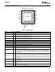

1
2
3
4
5
6
7
8
9 10 11 12 13 14 15 16
24
23
22
21
20
19
18
17
32 31 30 29 28 27 26 25
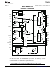
DIFFO
EN2/SS2/GSNS
ILIM2/VSNS
CS2–
CS2+
PG2
UVLO
ILIM1
CS1–
CS1+
PG1
VDD
BOOT1
SYNC
RT
EN1/SS1
FB1
COMP1
AGND
COMP2
FB2
TPS40322RHB
HDRV1
SW1
LDRV1
PGND1
BP6
PGND2
LDRV2
SW2
BOOT2
HDRV2
PHSET
TPS40322
SLUSAF8D –JUNE 2011–REVISED JANUARY 2014
www.ti.com
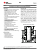
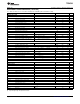
Table 1. PIN FUNCTIONS
NAME PIN I/O DESCRIPTION
AGND 6 – Low noise ground connection to the controller.
BOOT1 provides a bootstrapped supply for the high-side FET driver for channel 1 (CH1). Connect a
BOOT1 25 I
capacitor (0.1 μF typical) from BOOT1 to SW1 pin.
BOOT2 provides a bootstrapped supply for the high-side FET driver for channel 2 (CH2). Connect a
BOOT2 15 I
capacitor (0.1 μF typical) from BOOT2 to SW2 pin.
Output bypass for the internal regulator. Connect a low ESR bypass ceramic capacitor with a value of 3.3
BP6 20 O
μF or greater from this pin to the power ground plane.
COMP1 5 O Output of the error amplifier 1 and connection node for loop feedback components.
COMP2 7 O Output of the error amplifier 2 and connection node for loop feedback components.
CS1– 29 I Negative terminal of current sense amplifier for CH1
CS1+ 28 I Positive terminal of current sense amplifier for CH1
CS2– 12 I Negative terminal of current sense amplifier for CH2
CS2+ 13 I Positive terminal of current sense amplifier for CH2
Output of the differential amplifier. When the device is configured for dual channel mode, the DIFFO pin
DIFFO 9 O
must be either floating or tied to BP6
Logic level input which starts or stops CH1. Letting this pin float turns CH1 on. Pulling this pin low disables
CH1. This is also the soft-start programming pin. A capacitor connected from this pin to AGND programs
EN1/SS1 3 I the soft-start time. The capacitor is charged with an internal current source of 10 μA. The resulting voltage
ramp of this pin is also used as a second non-inverting input to the error amplifier 1 after a 0.8 V (typical)
level shift downwards.
Logic level input which starts or stops CH2. Letting this pin float turns CH2 on. Pulling this pin low disables
CH2. This is also the soft-start programming pin. A capacitor connected from this pin to AGND programs
the soft-start time. The capacitor is charged with an internal current source of 10 μA. The resulting voltage
EN2/SS2/GSNS 10 I
ramp of this pin is also used as a second non-inverting input to the error amplifier 2 after a 0.8 V (typical)
level shift downwards. In two-phase mode, this pin becomes GSNS as the negative terminal of a remote
sense amplifier.
Inverting input to the error amplifier. During normal operation, the voltage on this pin is equal to the internal
FB1 4 I
reference voltage.
Inverting input to the error amplifier. During normal operation, the voltage on this pin is equal to the internal
FB2 8 I reference voltage. Connecting the FB2 pin to the BP6 pin enables two-phase mode and disables the error
amplifier 2.
Bootstrapped gate drive output for the high-side N-channel MOSFET for CH1. A 2-Ω resistor is
HDRV1 24 O
recommended for a noisy environment.
10 Submit Documentation Feedback Copyright © 2011–2014, Texas Instruments Incorporated