
Datasheet


TPS40322
SLUSAF8D –JUNE 2011–REVISED JANUARY 2014
www.ti.com
These devices have limited built-in ESD protection. The leads should be shorted together or the device placed in conductive foam
during storage or handling to prevent electrostatic damage to the MOS gates.
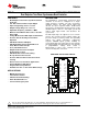
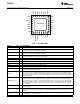
ORDERING INFORMATION
(1)
TEMPERATURE PINS PACKAGE ORDERING NUMBER
RANGE
–40°C to 125°C 32 QFN TPS40322RHB
(1) For the most current package and ordering information, see the Package Option Addendum at the end
of this document, or see the TI website at www.ti.com.
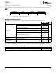
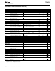
ABSOLUTE MAXIMUM RATINGS
(1)
Over operating free-air temperature range, all voltages are with respect to GND (unless otherwise noted)
VALUE
UNIT
MIN MAX
VDD –0.3 22
SW1, SW2 –3 27
SW1, SW2 (< 100 ns pulse width) –5
SW1, SW2 (< 10 ns pulse width) –7.5 30
BOOT1, BOOT2 –0.3 30
Voltage Range V
BOOT1, BOOT2 (< 10 ns pulse width) –0.5 33
BP6 –0.3 7
HDRV1, HDRV2 –2 30
BOOT1-SW1, BOOT2-SW2, HDRV1-SW1, HDRV2-SW2
–0.3 7
(differential from BOOT or HDRV to SW)
All other pins –0.3 7
T
J
Operating temperature –40 145 °C
Temperature
T
stg
Storage temperature –55 150 °C
Human Body Model (HBM) 2000 V
Electrostatic disharge
Charged Device Model (CDM) 1500 V
(1) Stresses beyond those listed under Absolute Maximum Ratings may cause permanent damage to the device. These are stress ratings
only, and functional operation of the device at these or any other conditions beyond those indicated under Recommended Operating
Conditions is not implied. Exposure to absolute maximum rated conditions for extended periods may affect device reliability.
RECOMMENDED OPERATING CONDITIONS
MIN MAX UNIT
V
VDD
Input operating voltage 3 20 V
T
J
Operating junction temperature –40 125 °C
2 Submit Documentation Feedback Copyright © 2011–2014, Texas Instruments Incorporated