
Datasheet


UDG-10216
22
21
30
28
13
14
8
7
CS2+
PG2
FB2
COMP2
LDRV1
PGND1
ILIM1
CS1+
27
4
5
2
1
32
10
SYNC
PHSET
EN2/SS2/GSNS
PG1
FB1
COMP1
RT
6AGND
3EN1/SS1
12CS2-
29CS1-
31
24
25
23
UVLO
HDRV1
BOOT1
SW1
18
19
11
LDRV2
PGND2
ILIM2/VSNS
16
15
17
HDRV2
BOOT2
SW2
20 BP6
26VDD
BP6
Linear
Regulator
Anti-Cross
Conduction
Logic
Anti-Cross
Conduction
+
OC
UV
OV
Detect
+
ISHARE
BP6
+
+
–
–
VREF
10 mA
+
–
–
VREF
10 mA
+
FB1
FB2
OV
UV
OC
Ramp
Generator
RAMP1
RAMP2
–
–
BP6
+
9DIFFO
RR
R
R
VSNS
GSNS
BP6
S
S
BG VREF
VDD
RAMP1
RAMP2
PWM2
PWM1
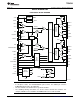
TPS40322
www.ti.com
SLUSAF8D –JUNE 2011–REVISED JANUARY 2014
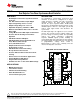
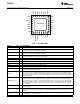
DEVICE INFORMATION
FUNCTIONAL BLOCK DIAGRAM
NOTE
• In two-phase mode, the EN2/SS2/GSNS pin becomes the GSNS pin and the
ILIM2/VSNS pin becomes the VSNS pin.
• The two channels are identical unless specified otherwise.
• The following naming conventions are used to better describe the functions. For
example, COMPx refers to COMP1 and COMP2, FBx refers to FB1 and FB2.
Copyright © 2011–2014, Texas Instruments Incorporated Submit Documentation Feedback 9