Using the PWR091EVM Dual-Output DC/DC Analog With PMBus Interface User's Guide Literature Number: SLVU638 January 2012
Contents 1 ......................................................................................................................... 7 ..................................................................................................... 7 1.2 Features .................................................................................................................. 7 Electrical Performance Specifications ................................................................................... 8 Schematic ........
www.ti.com List of Figures PWR091EVM Schematic 2 PWR091EVM Recommended Test Setup ............................................................................. 11 3 Texas Instruments USB-to-GPIO Adapter and Connections ........................................................ 12 4 Tip and Barrel Measurement ............................................................................................. 12 5 Efficiency of 1.2-V Output vs Line and Load ....................................................
www.ti.com 48 System Dashboard ........................................................................................................ 41 49 Display Change on Power Up ........................................................................................... 42 50 Faults Cleared 51 Status Screen .............................................................................................................. 43 52 Import Project / Import Configuration File ...........................................
www.ti.com List of Tables 1 PWR091EVM-001 Electrical Performance Specifications ............................................................. 8 2 The Functions of Each Test Points 3 4 5 6 6 ..................................................................................... Key Factory Configuration Parameters ................................................................................. List of Test Points for Loop Response Measurements ...........................................................
User's Guide SLVU638 – January 2012 Using the PWR091EVM Dual-Output DC/DC Analog With PMBus Interface The PWR091EVM evaluation module uses the TPS40422. The TPS40422 is a dual-channel, synchronous buck controller that operates from a nominal 4.5-V to 20-V supply. This controller is an analog PWM controller that allows programming and monitoring via the PMBus interface. It can be used as a dual, independent output or a dual-phase output controller.
Electrical Performance Specifications 2 www.ti.com Electrical Performance Specifications Table 1. PWR091EVM-001 Electrical Performance Specifications PARAMETER TEST CONDITIONS MIN TYP MAX 8 UNITS INPUT CHARACTERISTICS Voltage range VIN 12 14 Maximum input current VIN = 8 V, IO1 = 20 A, IO2 = 15 A 10 15 V No load input current VIN = 14 V, IO1 = 0 A, IO2 = 0 A 100 mA A OUTPUT CHARACTERISTICS VOUT1 Output voltage Output current = 10 A 1.
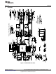
Schematic www.ti.com 3 Schematic Figure 1.
Test Setup www.ti.com 4 Test Setup 4.1 Test and Configuration Software To change any of the default configuration parameters on the EVM, it is necessary to obtain the TI Fusion Digital Power Designer software. 4.1.1 Description The Fusion Digital Power Designer is the graphical user interface (GUI) used to configure and monitor the Texas Instruments TPS40422 power controller on this evaluation module.
Test Setup www.ti.com As an example, if AWG 12 wire is used, no more than 3.15 feet of wire must be used between the EVM and the load. 4.3 Recommended Test Setup Figure 2.
Test Setup 4.4 www.ti.com USB Interface Adapter and Cable Figure 3. Texas Instruments USB-to-GPIO Adapter and Connections Figure 4. Tip and Barrel Measurement 4.
Test Setup www.ti.com Table 2. The Functions of Each Test Points Test Point Type Name Description TP1 T-H Loop PGOOD2 TP2 T-H Loop VIN TP3 T-H Loop VOUT1 Tip and barrel point for Vout 1. TP6 T-H Loop PGND Tip and barrel point for Vout 1 return. TP7 T-H Loop PGND General input voltage measurement. TP11 T-H Loop VOUT2 Tip and barrel point for Vout 2. TP13 T-H Loop AGND Return for PGOOD signals. TP14 T-H Loop PGND Tip and barrel point for Vout 2 return.
EVM Configuration Using the Fusion GUI 5 www.ti.com EVM Configuration Using the Fusion GUI The TPS40422 on this EVM leaves the factory pre-configured. See Table 3 for a short list of key factory configuration parameters as obtained from the configuration file. Table 3. Key Factory Configuration Parameters Address Hex 0x1B Address Dec Part ID 27 TPS40422 General Cmd ID With Phase Cmd Code Hex Encoded Hex Decoded Numeric VIN_OFF 0x36 0xF014 5.00 V 5 Turn OFF voltage VIN_ON 0x35 0xF01C 7.
Test Procedure www.ti.com NOTE: The IOUT_CAL_GAIN parameter is used by the TPS40422 in the calculation of output current level, and this number is the dc resistance of the output inductor. Although this number can be reconfigured, a number entry that does not match the actual DCR of the inductor on the EVM will result in current reporting inaccuracy. This also affects OC Fault and OC Warn performance.
Performance Data and Typical Characteristic Curves www.ti.com be limited to less than the switching frequency divided by 2 (Fsw/2). 6. For Vout2, connect the network analyzer’s isolation transformer from TP12 to TP10. 7. Connect the input signal measurement probe to TP12. Connect output signal measurement probe to TP10. 8. Connect the ground leads of both probe channels to TP4. 9. On the network analyzer, measure the Bode plot data as TP10/TP12 (Out/In).
Performance Data and Typical Characteristic Curves www.ti.com 7.1 Efficiency 100 VO = 1.2 V, 98 F SW = 300 kHz 96 VI = 12 V VI = 8 V 94 VI = 14 V 92 Efficiency - % 90 88 86 84 82 80 78 76 74 72 70 0 1 2 3 4 5 6 7 8 9 10 11 12 13 14 15 16 17 18 19 20 IO - Output Current - A Figure 5. Efficiency of 1.2-V Output vs Line and Load 100 VO = 3.
Performance Data and Typical Characteristic Curves 7.2 www.ti.com Load Regulation 1.2016 1.2015 VI = 8 V VO - Output Voltage - V 1.2014 VI = 14 V 1.2013 1.2012 VI = 12 V 1.2011 1.2010 1.2009 1.2008 1.2007 1.2006 0 1 2 3 4 5 6 7 8 9 10 11 12 13 14 15 16 17 18 19 20 IO - Output Current - A Figure 7. Load Regulation of 1.2-V Output 3.330 3.329 VO - Output Voltage - V 3.328 VI = 14 V VI = 12 V 3.327 3.326 VI = 8 V 3.325 3.324 3.323 3.
Performance Data and Typical Characteristic Curves www.ti.com Bode Plot 70 Gain - dB 60 140 8 V Phase 12 V Phase 14 V Phase 120 50 100 40 80 30 60 20 40 10 8 V Gain 12 V Gain 14 V Gain 20 0 Phase (Deg) 7.3 0 -10 -20 -20 -40 -30 100 1k 10k -60 100k f - Frequency - Hz Figure 9. Bode Plot of 1.
Performance Data and Typical Characteristic Curves 7.4 www.ti.com Transient Response Ch1 = Vout1 at 50mV/division, Ch2 = Iout1 at 5A/division Figure 11. Transient Response of 1.2-V Output at 8 Vin, Transient is 5 A to 11 A to 5 A Ch1 = Vout1 at 50mV/division, Ch2 = Iout1 at 5A/division Figure 12. Transient Response of 1.
Performance Data and Typical Characteristic Curves www.ti.com Ch1 = Vout2 at 20mV/division, Ch2 = Iout2 at 5A/division Figure 13. Transient Response of 3.3-V Output at 8 Vin, Transient is 5 A to 9 A to 5 A Ch1 = Vout2 at 20mV/division, Ch2 = Iout2 at 5A/division Figure 14. Transient Response of 3.
Performance Data and Typical Characteristic Curves 7.5 www.ti.com Output Ripple Ch1 = Vout1 at 20mV/division, Ch2 = SW Node at 10V/division Figure 15. Output Ripple and SW Node of 1.2-V Output at 8 Vin, 20-A Output Ch1 = Vout1 at 20mV/division, Ch2 = SW Node at 10V/division Figure 16. Output Ripple and SW Node of 1.
Performance Data and Typical Characteristic Curves www.ti.com Ch1 = Vout2 at 20mV/division, Ch2 = SW Node at 10V/division Figure 17. Output Ripple and SW Node of 3.3-V Output at 8 Vin, 15-A Output Ch1 = Vout2 at 20mV/division, Ch2 = SW Node at 10V/division Figure 18. Output Ripple and SW Node of 3.
Performance Data and Typical Characteristic Curves 7.6 www.ti.com HDRV and Switch Node Voltage Ch1 = SW Node at 5 V/division, Ch2 = HDRV at 5 V/division Figure 19. HDRV and SW Node of 1.2-V Output at 8 Vin, 20-A Output Ch1 = SW Node at 5 V/division, Ch2 = HDRV at 10 V/division Figure 20. HDRV and SW Node of 1.2-V Output at 12 Vin, 20-A Output Ch1 = SW Node at 5 V/division, Ch2 = HDRV at 5 V/division Figure 21. HDRV and SW Node of 3.
Performance Data and Typical Characteristic Curves www.ti.com Ch1 = SW Node at 5 V/division, Ch2 = HDRV at 10 V/division Figure 22. HDRV and SW Node of 3.3-V Output at 12 Vin, 15-A Output 7.7 Turnon Waveform Ch1 = Vout1 at 200 mV/division, Ch2 = Iout1 at 5 A/division, Ch3 = Vin at 5 V/division Ch2 (Iout) Inverted to better display V and I. Figure 23. Turnon Waveform of 1.2-V Output at 8-V, 12-V and 14-V Input, 20-A Output Ch1 = Vout1 at 200 mV/division, Ch3 = Vin at 5 V/division Figure 24.
EVM Assembly Drawing and PCB Layout www.ti.com Ch1 = Vout2 at 500 mV/division, Ch2 = Iout2 at 5 A/division, Ch3 = Vin at 5 V/division Ch2 (Iout) Inverted to better display V and I. Figure 25. Turnon Waveform of 3.3-V Output at 8-V, 12-V, and 14-V Input, 15-A Output Ch1 = Vout1 at 500 mV/division, Ch3 = Vin at 5 V/division Figure 26. Turnon Waveform of 3.
EVM Assembly Drawing and PCB Layout www.ti.com Figure 27.
EVM Assembly Drawing and PCB Layout www.ti.com Figure 28.
EVM Assembly Drawing and PCB Layout www.ti.com Figure 29.
EVM Assembly Drawing and PCB Layout www.ti.com Figure 30.
EVM Assembly Drawing and PCB Layout www.ti.com Figure 31.
EVM Assembly Drawing and PCB Layout www.ti.com Figure 32.
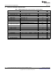
Bill of Materials www.ti.com 9 Bill of Materials The EVM components list according to the schematic shown in . Table 6. PWR091 Bill of Materials Qty Reference Designator Description Manufacturer Part Number 2 C23 C27 0.47uF, Ceramic, 16V, X5R, 10%, 0402 STD STD 3 C1 C5 C9 0.1uF, Ceramic, 50V, X7R, 10%, 0603 STD STD 3 C10-12 1.0uF, Ceramic, 25V, X7R, 10%, 0603 STD STD 2 C21 C25 1.
Screen Shots 10 www.ti.com Screen Shots 10.1 Fusion GUI Screen Shots Figure 33. First Window at Fusion Launch Device Found Figure 34. Scan Finds Device Successfully Figure 35.
Screen Shots www.ti.com Figure 36. Software Launch Continued Use this screen to configure (Figure 37): • OC Fault and OC Warn • OT Fault and OT Warn • Power Good Limits • Fault response • UVLO • On/Off Config • Soft Start time • Margin voltage Figure 37.
Screen Shots • www.ti.com Iout Cal Gain (DCR of output choke) Figure 38. Configure- Other Use this screen to configure all of the configurable parameters (Figure 39). The screen also shows other details like hexadecimal (hex) encoding. Figure 39. Configure- All Changing the On/Off Config prompts a pop-up window with details of the options Figure 40).
Screen Shots www.ti.com Figure 40. Configure- Limits and On/Off- On/Off Config Pop-up After a change is selected, orange U icon is displayed to offer Undo Change option. Change is not retained until either Write to Hardware or Store User Defaults is selected. When Write to Hardware is selected, change is committed to volatile memory and defaults back to previous setting on input power cycle.
Screen Shots www.ti.com The Iout Cal Gain can be typed in or scrolled to a new value. The range for Iout Cal Gain is 0.244 mΩ to 15.5 mΩ and the resolution step is 30.5 µΩ. If a value is typed in that is between the available discrete steps, the typed-in value does not change but the nearest discrete step is retained. The actual step is displayed on relaunch of the Fusion GUI (Figure 42). Figure 42.
Screen Shots www.ti.com After making changes to one or more configurable parameters, the changes can be committed to nonvolatile memory by selecting Store User Defaults. This action prompts a confirm selection pop-up, and if confirmed, the changes are committed to nonvolatile memory (Figure 44). Figure 44. Configure- Store User Defaults A scroll-down menu in the upper right corner can be selected to change the view screens to one output rail or the other(Figure 45). Figure 45.
Screen Shots www.ti.com In the lower left corner, the different view screens can be changed. The view screens can be changed between Configure, Monitor and Status as needed (Figure 46). Figure 46. Change View Screen to Monitor Screen When the Monitor screen is selected (Figure 47), the screen changes to display real-time data of the parameters that are measured by the controller. This screen provides access to: • Graphs of Vout, Iout, Temperature, and Pout. As shown, Pout display is turned off.
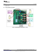
Screen Shots www.ti.com Figure 47. Monitor Screen Selecting System Dashboard from mid-left screen adds a new window which displays system-level information (Figure 48). Figure 48.
Screen Shots www.ti.com When the EVM starts converting power, the Vout graph changes scale to display both the zero and Vout level. Only one rail can be displayed on the graphs at any time, but the other rail voltage, current, power, and temperature are displayed in the upper left window. Once the EVM is converting and clear of any faults, selecting Clear Faults clears any prior fault flags (Figure 49). Figure 49. Display Change on Power Up Selecting Clear Faults clears any prior fault flags.
Screen Shots www.ti.com Selecting Status from lower left corner shows the status of the controller (Figure 51). Figure 51. Status Screen Selecting the pull-down menu File- Import Project from the upper left menu bar can be used to configure all parameters in the device at once with a desired configuration, or even revert back to a known-good configuration. This action results in a browse-type sequence where the desired config file can be located and loaded (Figure 52). Figure 52.
Screen Shots www.ti.com Selecting Store User Configuration to Flash Memory from the Device pull-down menu has the same functionality as the Store User Defaults button from within the Configure screen. It results in committing the current configuration to nonvolatile memory (Figure 53). Figure 53. Store Config To Memory Selecting Data Logging (Figure 54) from the Tools drop-down menu enables the logging of common operating values such as Vout, Iout, and Temperature for both output rails.
Screen Shots www.ti.com Select the storage location for the file and the type of file. As shown (Figure 55), the file will be a CSV file to be stored in the directory path shown. Logging begins when the Start Data Logging button is selected, and stops when it is reselected (as Stop Data Logging). Figure 55. Data Logging Details Data is stored in a CSV file, with date-stamp name (Figure 56). Figure 56. Data Log Common contents of the data log.
Screen Shots www.ti.com Figure 57. Data Log File Selecting PMBus Logging (Figure 58) from the Tools drop-down menu enables the logging of all PMBus activity. This includes communications traffic for each polling loop between the GUI and the device. It also includes common operating values such as Vout, Iout, and Temperature for both output rails. The user is prompted to select a location for the file to be stored. See next screen (Figure 59). Figure 58.
Screen Shots www.ti.com Select the storage location for the file and the type of file. As shown (Figure 59), the file is a CSV file to be stored in the directory path shown. Logging begins when the Start Logging button is selected, and stops when it is reselected (as Stop Logging). This file can rapidly grow in size, so caution is advised when using this function. Figure 59. PMBus Log Details Data is stored in a CSV file, with date-stamp name (Figure 60). Figure 60.
Screen Shots www.ti.com Figure 61.
Evaluation Board/Kit Important Notice Texas Instruments (TI) provides the enclosed product(s) under the following conditions: This evaluation board/kit is intended for use for ENGINEERING DEVELOPMENT, DEMONSTRATION, OR EVALUATION PURPOSES ONLY and is not considered by TI to be a finished end-product fit for general consumer use. Persons handling the product(s) must have electronics training and observe good engineering practice standards.
EVALUATION BOARD/KIT/MODULE (EVM) ADDITIONAL TERMS Texas Instruments (TI) provides the enclosed Evaluation Board/Kit/Module (EVM) under the following conditions: The user assumes all responsibility and liability for proper and safe handling of the goods. Further, the user indemnifies TI from all claims arising from the handling or use of the goods.
FCC Interference Statement for Class B EVM devices This equipment has been tested and found to comply with the limits for a Class B digital device, pursuant to part 15 of the FCC Rules. These limits are designed to provide reasonable protection against harmful interference in a residential installation. This equipment generates, uses and can radiate radio frequency energy and, if not installed and used in accordance with the instructions, may cause harmful interference to radio communications.
【Important Notice for Users of this Product in Japan】 】 This development kit is NOT certified as Confirming to Technical Regulations of Radio Law of Japan If you use this product in Japan, you are required by Radio Law of Japan to follow the instructions below with respect to this product: 1. 2. 3. Use this product in a shielded room or any other test facility as defined in the notification #173 issued by Ministry of Internal Affairs and Communications on March 28, 2006, based on Sub-section 1.
EVALUATION BOARD/KIT/MODULE (EVM) WARNINGS, RESTRICTIONS AND DISCLAIMERS For Feasibility Evaluation Only, in Laboratory/Development Environments. Unless otherwise indicated, this EVM is not a finished electrical equipment and not intended for consumer use.
IMPORTANT NOTICE Texas Instruments Incorporated and its subsidiaries (TI) reserve the right to make corrections, enhancements, improvements and other changes to its semiconductor products and services per JESD46, latest issue, and to discontinue any product or service per JESD48, latest issue. Buyers should obtain the latest relevant information before placing orders and should verify that such information is current and complete.