
Datasheet


1
1
+
+
C1
C12
C6
C7
C9
C8
C10
C11
J5
J1
J3
J7
J4
JP1
L1
R8
R14
R12
R13
R1
R9
R7
R5
R6
R11
R2
R10
R15
J2
TP1
TP3
TP6
TP7
TP2
TP5
TP4
U1
Q1
R3
R4
C16
TP8
C13
C15
C14
C2
C3
C4
J6
TP9
R16
R17
C5
+
+
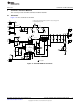
PWR198 Rev. A
ON
OFF
EN
VBIAS
VIN =
GND
6V-12.6V
VIN
GND
VOUT =
15V @ 2A
VOUTGND
GND
PGOOD
HDRV
PGND
VOUT
LOOP
LDRV
SW
(OPTIONAL)
TPS43061EVM-198
C1
C12
C6
C7
C9
C8
C10
C11
J5
J1
J3
J7
J4
JP1
L1
R8
R14
R12
R13
R1
R9
R7
R5
R6
R11
R2
R10
R15
J2
TP1
TP3
TP6
TP7
TP2
TP5
TP4
U1
Q1
R3
R4
C16
TP8
C13
C15
C14
C2
C3
C4
J6
TP9
R16
R17
C5
www.ti.com
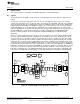
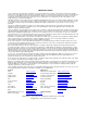
Board Layout
4 Board Layout
This section provides a description of the EVM, board layout, and layer illustrations.
4.1 Layout
The board layout for the EVM is shown in Figure 18 through Figure 22. This design has 4 layers of 2-oz
copper.
The top layer contains the main power traces for V
IN
, V
OUT
, and SW. Also on the top layer are all other
components to allow the user to easily view, probe, and evaluate the TPS43061 control IC. The remaining
area is filled with ground. The remaining three layers have additional copper for VIN, VOUT, AGND, and
PGND connected with multiple vias. Additional copper is also connected to the sense resistor to aid with
thermal dissipation. The second internal layer and bottom layer contain signal routes. Five vias directly
under the TPS43061 device provide a thermal path from the top-side ground plane to the bottom-side and
internal AGND plane. Lastly, the layout guidelines should be followed for the CSD86330Q3D which
includes 12 vias beneath the device to the internal and bottom PGND planes to aid with thermal
dissipation.
All noise-sensitive analog circuitry are placed as close as possible to the IC. The voltage divider network
ties to the output voltage at the point of regulation on the bottom layer, near the output capacitors. Q1 is
also placed as close as possible to the IC to keep the gate-drive traces as short as possible. The output
capacitors are placed next to Q1 to limit the length of the high frequency switching current path. The SW
copper is kept as small as possible to limit radiated noise from the high-frequency switching voltage node.
The power pad is connected to the AGND pin and all noise-sensitive circuitry must use this as the ground
return path. The ground return for the power components are connected to the PGND pin. The AGND and
PGND are connected at one point near the PGND pin. The bypass capacitors for VIN and VCC are placed
next to their respective pins. The filter capacitor between ISNS+ and ISNS- is located next to the pins to
help filter out switching noise. An additional input bulk capacitor may be required (C13) depending on the
connection to the EVM from the input supply. See the product datasheet for all layout recommendations.
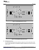
Figure 18. TPS43061EVM-198 Top Assembly and Silkscreen
13
SLVU799A–November 2012–Revised March 2013 Using the TPS43061 Boost Evaluation Module (EVM)
Submit Documentation Feedback
Copyright © 2012–2013, Texas Instruments Incorporated