
Datasheet


70
75
80
85
90
95
100
0 0.5 1 1.5 2 2.5 3 3.5 4 4.5
Efficiency - %
Output Current - A
Vin = 6V
Vin = 9V
Vin = 12V
C001
V
OUT
= 15 V, fsw = 750 kHz
Test Setup and Results
www.ti.com
Table 3. EVM Connectors and Test points (continued)
Reference Designator Function
TP1 PGOOD test point for power good output voltage indicator
TP2 HDRV test point for high-side gate-drive voltage
TP3 V
OUT
test point at V
OUT
connector
TP4 GND test point at V
OUT
connector
TP5 SW test point for switch node voltage
TP6 Test point between voltage divider network and output used for loop response measurements.
TP7 LDRV test point for low-side gate-drive voltage
TP8 V
IN
test point at V
IN
connector
TP9 GND test point at V
IN
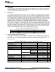
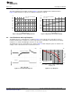
2.2 Efficiency
The efficiency of this EVM peaks at a load current of about 2 A with V
IN
= 12 V, and then decreases as the
load current increases towards maximum load. Figure 2 shows the efficiency for the EVM brought to
current limit for each input voltage. Dotted-line efficiency data was measured with Wurth Elektroniks
744311330. Measurements are taken at ambient temperature of 25°C. The efficiency may be lower at
higher ambient temperatures due to temperature variation in the drain-to-source resistance of the selected
external MOSFETs.
Figure 2. Efficiency Versus Load Current
6
Using the TPS43061 Boost Evaluation Module (EVM) SLVU799A–November 2012–Revised March 2013
Submit Documentation Feedback
Copyright © 2012–2013, Texas Instruments Incorporated