TPS43330-Q1 TPS43332-Q1 www.ti.
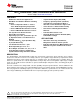
TPS43330-Q1 TPS43332-Q1 SLVSA82E – MARCH 2011 – REVISED APRIL 2013 www.ti.com VBAT VBUCKA VBuckA VBAT TPS43330-Q1 or TPS43332-Q1 VBUCKB VBuckB 2V Figure 1. Typical Application Diagram These devices have limited built-in ESD protection. The leads should be shorted together or the device placed in conductive foam during storage or handling to prevent electrostatic damage to the MOS gates.
TPS43330-Q1 TPS43332-Q1 www.ti.com SLVSA82E – MARCH 2011 – REVISED APRIL 2013 space ABSOLUTE MAXIMUM RATINGS (1) Voltage MIN MAX Input voltage: VIN, VBAT –0.3 60 V Ground: PGNDA–AGND, PGNDB–AGND –0.3 0.3 V Enable inputs: ENA, ENB –0.3 60 V Bootstrap inputs: CBA, CBB –0.3 68 V Bootstrap inputs: CBA–PHA, CBB–PHB –0.3 8.8 V Phase inputs: PHA, PHB –0.7 60 V –1 60 V Feedback inputs: FBA, FBB –0.3 13 V Error amplifier outputs: COMPA, COMPB –0.
TPS43330-Q1 TPS43332-Q1 SLVSA82E – MARCH 2011 – REVISED APRIL 2013 www.ti.com THERMAL INFORMATION TPS4333x-Q1 THERMAL METRIC (1) DAP UNIT 38 PINS Junction-to-ambient thermal resistance (2) θJA (3) 27.3 °C/W θJCtop Junction-to-case (top) thermal resistance 19.6 °C/W θJB Junction-to-board thermal resistance (4) 15.9 °C/W ψJT Junction-to-top characterization parameter (5) 0.24 °C/W ψJB Junction-to-board characterization parameter (6) 6.
TPS43330-Q1 TPS43332-Q1 www.ti.com SLVSA82E – MARCH 2011 – REVISED APRIL 2013 DC ELECTRICAL CHARACTERISTICS VIN = 8 V to 18 V, TJ = –40°C to 150°C (unless otherwise noted) NO. PARAMETER 1.0 Input Supply 1.1 VBAT 1.2 1.3 1.4 VIN VIN(UV) VBOOST_UNLOC TEST CONDITIONS MIN Boost controller enabled, after satisfying initial start-up condition Supply voltage Input voltage required for device on initial start-up Boost unlock threshold VIN falling.
TPS43330-Q1 TPS43332-Q1 SLVSA82E – MARCH 2011 – REVISED APRIL 2013 www.ti.com DC ELECTRICAL CHARACTERISTICS (continued) VIN = 8 V to 18 V, TJ = –40°C to 150°C (unless otherwise noted) NO. PARAMETER 4.0 Boost Controller 4.1 Vboost7V 4.2 4.3 4.4 Vboost7V-th Vboost10V Vboost10V-th 4.5 Vboost11V 4.6 Vboost11V-th TEST CONDITIONS MIN TYP MAX Boost VOUT = 7 V DIV = low, VBAT = 2 V to 7 V 6.8 7 7.3 Boost-enable threshold Boost VOUT = 7 V, VBAT falling 7.5 8 8.
TPS43330-Q1 TPS43332-Q1 www.ti.com SLVSA82E – MARCH 2011 – REVISED APRIL 2013 DC ELECTRICAL CHARACTERISTICS (continued) VIN = 8 V to 18 V, TJ = –40°C to 150°C (unless otherwise noted) NO. PARAMETER TEST CONDITIONS MIN TYP MAX UNIT High-Side External NMOS Gate Drivers for Buck Controller 5.11 IGX1_peak Gate-driver peak current 5.12 rDS(on) Source and sink driver 1.5 VREG = 5.8 V, IGX1 current = 200 mA A 2 Ω 2 Ω Low-Side NMOS Gate Drivers for Buck Controller 5.
TPS43330-Q1 TPS43332-Q1 SLVSA82E – MARCH 2011 – REVISED APRIL 2013 www.ti.com DC ELECTRICAL CHARACTERISTICS (continued) VIN = 8 V to 18 V, TJ = –40°C to 150°C (unless otherwise noted) NO. PARAMETER TEST CONDITIONS 12.0 Power Good / Delay 12.1 PGpullup Pullup for A and B to Sx2 12.2 PGth1 Power-good threshold 12.3 PGhys Hysteresis 12.4 PGdrop Voltage drop –5% –7% MAX UNIT kΩ –9% 2% 12.6 PGleak Power-good leakage 12.
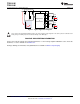
TPS43330-Q1 TPS43332-Q1 www.ti.com SLVSA82E – MARCH 2011 – REVISED APRIL 2013 DEVICE INFORMATION DAP PACKAGE (TOP VIEW) VBAT 1 38 DS 2 37 GC1 3 36 DIV GC2 4 35 VREG CBA 5 34 CBB GA1 6 33 GB1 PHA 7 32 PHB GA2 8 31 9 30 SA1 10 29 SB1 SA2 11 28 SB2 FBA 12 27 13 26 SSA 14 25 SSB PGA 15 24 PGB PGNDA COMPA VIN EXTSUP GB2 PGNDB FBB COMPB ENA 16 23 AGND ENB 17 22 RT 18 21 DLYAB 19 20 SYNC COMPC ENC PIN FUNCTIONS NO.
TPS43330-Q1 TPS43332-Q1 SLVSA82E – MARCH 2011 – REVISED APRIL 2013 www.ti.com PIN FUNCTIONS (continued) NAME NO. I/O DESCRIPTION ENB 17 I Enable input for BuckB (active-high with an internal pullup current source). An input voltage higher than 1.7 V enables the controller, whereas an input voltage lower than 0.7 V disables the controller. When both ENA and ENB are low, the device shuts down and consumes less than 4 µA of current. NOTE: DIV = high and ENC = high inhibits low-power mode on the bucks.
TPS43330-Q1 TPS43332-Q1 www.ti.com SLVSA82E – MARCH 2011 – REVISED APRIL 2013 PIN FUNCTIONS (continued) NAME SSB NO. 25 I/O DESCRIPTION O Soft-start or tracking input for buck controller BuckB. The buck controller regulates the FBB voltage to the lower of 0.8 V or the SSB pin voltage. An internal pullup current source of 1 µA is present at the pin, and an appropriate capacitor connected here sets the soft-start ramp interval.
TPS43330-Q1 TPS43332-Q1 SLVSA82E – MARCH 2011 – REVISED APRIL 2013 VIN EXTSUP VREG SYNC Duplicate for second Buck controller channel Internal ref (Band gap) 38 Gate Driver Supply 37 PWM Logic 5 CBA 6 GA1 7 PHA 8 GA2 9 PGNDA 10 SA1 11 SA2 12 FBA 13 COMPA 15 PGA 21 DLYAB 34 CBB 33 GB1 32 PHB 31 GB2 30 PGNDB 29 SB1 28 SB2 27 FBB 26 COMPB 24 PGB VREG 35 Internal Oscillator 22 180 deg RT www.ti.
TPS43330-Q1 TPS43332-Q1 www.ti.com SLVSA82E – MARCH 2011 – REVISED APRIL 2013 TYPICAL CHARACTERISTICS EFFICIENCY ACROSS OUTPUT CURRENTS (BUCKS) INDUCTOR CURRENTS (BUCK) VIN = 12 V, VOUT = 5 V, SWITCHING FREQUENCY = 400 kHz INDUCTOR = 4.7 µH, RSENSE = 10 mW VIN = 12 V, VOUT = 5 V, SWITCHING FREQUENCY = 400 kHz INDUCTOR = 4.
TPS43330-Q1 TPS43332-Q1 SLVSA82E – MARCH 2011 – REVISED APRIL 2013 www.ti.com TYPICAL CHARACTERISTICS (continued) LOAD STEP RESPONSE (BOOST) (0 TO 5 A AT 10 A/µs) EFFICIENCY ACROSS OUTPUT CURRENTS (BOOST) VBAT (BOOST INPUT) = 5 V, VIN (BOOST OUTPUT) = 10 V, SWITCHING FREQUENCY = 200 KHz, INDUCTOR = 680 nH, RSENSE = 10 m , CIN = 440 F, COUT = 660 F VIN (BOOST OUTPUT) = 10 V, SWITCHING FREQUENCY = 200 kHz, INDUCTOR = 1 µH, RSENSE = 7.
TPS43330-Q1 TPS43332-Q1 www.ti.com SLVSA82E – MARCH 2011 – REVISED APRIL 2013 TYPICAL CHARACTERISTICS (continued) NO-LOAD QUIESCENT CURRENT versus TEMPERATURE BUCKx PEAK CURRENT LIMIT versus COMPx VOLTAGE 75 Peak Current Sense Voltage (mV) Quiescent Current (µA) 60 50 BOTH BUCKS ON 40 30 ONE BUCK ON 20 10 NEITHER BUCK ON 0 -40 -15 10 85 35 60 Temperature (°C) 110 135 62.5 50 37.5 25 12.5 SYNC = LOW 0 –12.5 –25 SYNC = HIGH –37.5 0.65 160 0.8 0.95 CURRENT-SENSE PINS INPUT CURRENT (BUCK) 0.
TPS43330-Q1 TPS43332-Q1 SLVSA82E – MARCH 2011 – REVISED APRIL 2013 www.ti.com DETAILED DESCRIPTION BUCK CONTROLLERS: NORMAL MODE PWM OPERATION Frequency Selection and External Synchronization The buck controllers operate using constant-frequency peak-current-mode control for optimal transient behavior and ease of component choices. The switching frequency is programmable between 150 kHz and 600 kHz, depending upon the resistor value at the RT pin.
TPS43330-Q1 TPS43332-Q1 www.ti.com SLVSA82E – MARCH 2011 – REVISED APRIL 2013 Current-Mode Operation Peak-current-mode control regulates the peak current through the inductor to maintain the output voltage at its set value. The error between the feedback voltage at FBx and the internal reference produces a signal at the output of the error amplifier (COMPx) which serves as the target for the peak inductor current.
TPS43330-Q1 TPS43332-Q1 SLVSA82E – MARCH 2011 – REVISED APRIL 2013 www.ti.com Slope Compensation Optimal slope compensation, which is adaptive to changes in input voltage and duty cycle, allows stable operation under all conditions. For optimal performance of this circuit, choose the inductor and sense resistor according to the following: L ´ f SW = 200 RS where L is the buck-regulator inductor in henries. RS is the sense resistor in ohms. fsw is the buck-regulator switching frequency in hertz.
TPS43330-Q1 TPS43332-Q1 www.ti.com SLVSA82E – MARCH 2011 – REVISED APRIL 2013 The TPS43330-Q1 and TPS43332-Q1 can support the full-current load during low-power mode until the transition to normal mode takes place. The design ensures that exit of the low-power mode occurs at 10% (typical) of full-load current if the selection of inductor and sense resistor is as recommended. Moreover, there is always a hysteresis between the entry and exit thresholds to avoid oscillating between the two modes.
TPS43330-Q1 TPS43332-Q1 SLVSA82E – MARCH 2011 – REVISED APRIL 2013 www.ti.com VBAT VIN TPS43330-Q1 or TPS43332-Q1 GC1 DS RIFLT CIFLT RISEN Figure 22. External Current Shunt Resistor Frequency-Hopping Spread Spectrum The TPS43332-Q1 features a frequency-hopping pseudo-random spectrum-spreading architecture. On this device, whenever the SYNC pin is high, the internal oscillator frequency varies from one cycle to the next within a band of ±5% around the value programmed by the resistor at the RT pin.
TPS43330-Q1 TPS43332-Q1 www.ti.com SLVSA82E – MARCH 2011 – REVISED APRIL 2013 Table 2.
TPS43330-Q1 TPS43332-Q1 SLVSA82E – MARCH 2011 – REVISED APRIL 2013 www.ti.com During low-power mode, the EXTSUP functionality is not available. The internal regulator operates as a shunt regulator powered from VIN and has a typical value of 7.5 V. Current-limit protection for VREG is available in low-power mode as well. If EXTSUP is unused, leave the pin open without a capacitor installed.
TPS43330-Q1 TPS43332-Q1 www.ti.com SLVSA82E – MARCH 2011 – REVISED APRIL 2013 With the boost controller enabled, a voltage less than 1.9 V (typical) on VBAT triggers an undervoltage lockout and pulls the boost gate driver (GC1) low (this action has a filter delay of 5 µs, typical). As a result, VIN falls at a rate dependent on its capacitor and load, eventually triggering VIN undervoltage. A short falling transient at VBAT even lower than 2 V can thus be survived, if VBAT returns above 2.
TPS43330-Q1 TPS43332-Q1 SLVSA82E – MARCH 2011 – REVISED APRIL 2013 www.ti.com APPLICATION INFORMATION The following example illustrates the design process and component selection for the TPS43330-Q1. Table 3 lists the design-goal parameters. Table 3. Application Example PARAMETER VBuckA VBuckB BOOST VIN = 6 V to 30 V 12 V - typical VIN = 6 V to 30 V 12 V - typical VBAT = 5 V (cranking pulse input) to 30 V Output voltage, VOUTx 5V 3.3 V 10 V Maximum output current, IOUTx 3A 2A 2.5 A ±0.
TPS43330-Q1 TPS43332-Q1 www.ti.com SLVSA82E – MARCH 2011 – REVISED APRIL 2013 Boost Maximum Input Current IIN_MAX The maximum input current flows at the minimum input voltage and maximum load. The efficiency for VBAT = 5 V at 2.5 A is 80%, based on the typical characteristics plot. POUT 25 W PINmax = = = 31.3 W Efficiency 0.8 Hence, IINmax (at VBAT = 5 V) = 31.3 W = 6.3 A 5V Boost Inductor Selection, L Allow input ripple current of 40% of IIN max at VBAT = 5 V.
TPS43330-Q1 TPS43332-Q1 SLVSA82E – MARCH 2011 – REVISED APRIL 2013 www.ti.com Output Capacitor, COUTx To ensure stability, choose output capacitor COUTx such that fRHP fLC £ 10 10 2p ´ L ´ COUTx £ V BAT min 2p ´ IINmax ´ L æ 10 ´ IINmax ³ç ç VBAT min è COUTx 2 2 ö æ 10 ´ 6.3 A ö ÷ ´L = ç ÷ ´ 4 mH ÷ 5V è ø ø COUTx min ³ 635 mF Select COUTx = 680 µF. This capacitor is usually aluminum electrolytic with ESR in the tens of milliohms.
TPS43330-Q1 TPS43332-Q1 www.ti.com SLVSA82E – MARCH 2011 – REVISED APRIL 2013 Output Ripple Voltage Due to Load Transients, ∆VOUTx Assume a bandwidth of fC = 10 kHz. DVOUTx = R ESR ´ DI OUTx + = 0.04 W ´ 2.5 A + DI OUTx 4 ´ COUTx ´ f C 2.5 A = 0.19 V 4 ´ 660 mF ´ 10 kHz Because the boost converter is active only during brief events such as a cranking pulse, and the buck converters are high-voltage tolerant, a higher excursion on the boost output may be tolerable in some cases.
TPS43330-Q1 TPS43332-Q1 SLVSA82E – MARCH 2011 – REVISED APRIL 2013 www.ti.com Output Schottky Diode D1 Selection Maximizing efficiency requires a Schottky diode with low forward-conducting voltage VF over temperature and fast switching characteristics. The reverse breakdown voltage should be higher than the maximum input voltage, and the component should have low reverse leakage current. Additionally, the peak forward current should be higher than the peak inductor current.
TPS43330-Q1 TPS43332-Q1 www.ti.com SLVSA82E – MARCH 2011 – REVISED APRIL 2013 Current-Sense Resistor RSENSE Based on the typical characteristics for the VSENSE limit with VIN versus duty cycle, the sense limit is approximately 65 mV (at VIN = 12 V and duty cycle of 5 V / 12 V = 0.416). Allowing for tolerances and ripple currents, choose a VSENSE maximum of 50 mV. 50 mV RSENSE = = 17 mW 3A Select 15 mΩ.
TPS43330-Q1 TPS43332-Q1 SLVSA82E – MARCH 2011 – REVISED APRIL 2013 www.ti.com Selection of Components for Type II Compensation VOUT RESR RL R1 VSENSE GmBUCK COUT R2 VREF COMP Type 2A R3 R0 C2 C1 Figure 27. Buck Compensation Components R3 = 2p ´ f C ´ VOUT ´ COUTx = 2p ´ 50 kHz ´ 5 V ´ 100μF GmBUCK ´ K CFB ´ VREF GmBUCK ´ K CFB ´ VREF = 23.57 kW where VOUT = 5 V, COUT = 100 µF, GmBUCK = 1 mS, VREF = 0.8 V, KCFB = 0.125 / RSENSE = 8.33 S (0.
TPS43330-Q1 TPS43332-Q1 www.ti.com SLVSA82E – MARCH 2011 – REVISED APRIL 2013 Resistor Divider Selection for Setting VOUTA Voltage b= VREF 0.8 V = = 0.16 VOUTA 5V Choose the divider current through R1 and R2 to be 50 µA. Then R1 + R2 = 5V 50 mA = 66 kW and R2 R1 + R2 = 0.16 Therefore, R2 = 16 kΩ and R1 = 84 kΩ. BuckB Component Selection Using the same method as for VBuckA produces the following parameters and components. VOUTB 3.
TPS43330-Q1 TPS43332-Q1 SLVSA82E – MARCH 2011 – REVISED APRIL 2013 www.ti.com C1 C2 = æ fSW ö ÷ -1 è 2 ø 2p ´ R3 ´ C1´ ç = fC = = 1.1nF æ 400 kHz ö 2p ´ 30 kW ´ 1.1nF ´ ç ÷ -1 2 è ø GmBUCK ´ R3 ´ K CFB ´ 2p ´ COUTB = 27 pF VREF VOUTB 1mS ´ 30 kW ´ 4.16 S ´ 0.8 V 2p ´ 100 μF ´ 3.3 V = 48 kHz fC is close to the target bandwidth of 50 kHz. The resulting zero frequency fZ1 fZ1 = 1 1 = 2p ´ R3 ´ C1 = 4.8 kHz 2p ´ 30 kW ´ 1.1nF fZ1 is close to the fC guideline of 5 kHz.
TPS43330-Q1 TPS43332-Q1 www.ti.com SLVSA82E – MARCH 2011 – REVISED APRIL 2013 BuckX High-Side and Low-Side N-Channel MOSFETs An internal supply, which is 5.8 V typical under normal operating conditions, provides the gate-drive supply for these MOSFETs. The output is a totem pole, allowing full-voltage drive of VREG to the gate with peak output current of 1.5 A.
TPS43330-Q1 TPS43332-Q1 SLVSA82E – MARCH 2011 – REVISED APRIL 2013 www.ti.com Schematics The following section summarizes the previously calculated example and gives schematic and component proposals. Table 4. Application Example 1 PARAMETER VBuckA VBuckB BOOST VIN = 6 V to 30 V 12 V - typical VIN = 6 V to 30 V 12 V - typical VBAT = 5 V (cranking pulse input) to 30 V Output voltage, VOUTx 5V 3.3 V 10 V Maximum output current, IOUTx 3A 2A 2.
TPS43330-Q1 TPS43332-Q1 www.ti.com SLVSA82E – MARCH 2011 – REVISED APRIL 2013 Table 6. Application Example 2 PARAMETER Input voltage VBuckA VBuckB BOOST VIN = 5 V to 30 V 12 V - typical VIN = 6 V to 30 V 12 V - typical VBAT = 5 V (cranking pulse input) to 30V 10 V Output voltage, VOUTx 5V 3.3 V Maximum output current, IOUTx 2.7 A 5A 3A Load-step output tolerance, ∆VOUT + ∆VOUT(Ripple) ±0.2 V ±0.12 V ±0.5 V 0.1 A to 2.7 A 0.1 A to 5 A 0.
TPS43330-Q1 TPS43332-Q1 SLVSA82E – MARCH 2011 – REVISED APRIL 2013 www.ti.com Table 8. Application Example 3 PARAMETER VBuckA VBuckB BOOST VIN = 5 V to 30 V 12 V - typical VIN = 6 V to 30 V 12 V - typical VBAT = 5 V (cranking pulse input) to 30 V Output voltage, VOUTx 5V 2.5 V 10 V Maximum output current, IOUTx 3A 1A 2A ±0.2 V ±0.12 V ±0.5 V 0.1 A to 3 A 0.1 A to 1 A 0.
TPS43330-Q1 TPS43332-Q1 www.ti.com SLVSA82E – MARCH 2011 – REVISED APRIL 2013 Power Dissipation Derating Profile, 38-Pin HTTSOP PowerPAD™ Package Figure 31. Derating Profile for Power Dissipation Based on High-K JEDEC PCB PCB Layout Guidelines Grounding and PCB Circuit Layout Considerations Boost converter 1. The path formed from the input capacitor to the inductor and BOT_SW3 with the low-side current-sense resistor should have short leads and PC trace lengths.
TPS43330-Q1 TPS43332-Q1 SLVSA82E – MARCH 2011 – REVISED APRIL 2013 www.ti.
PACKAGE OPTION ADDENDUM www.ti.
PACKAGE MATERIALS INFORMATION www.ti.com 25-Dec-2013 TAPE AND REEL INFORMATION *All dimensions are nominal Device Package Package Pins Type Drawing SPQ Reel Reel A0 Diameter Width (mm) (mm) W1 (mm) TPS43330QDAPRQ1 HTSSOP DAP 38 2000 330.0 24.4 TPS43332QDAPRQ1 HTSSOP DAP 38 2000 330.0 24.4 Pack Materials-Page 1 B0 (mm) K0 (mm) P1 (mm) W Pin1 (mm) Quadrant 8.6 13.0 1.8 12.0 24.0 Q1 8.6 13.0 1.8 12.0 24.
PACKAGE MATERIALS INFORMATION www.ti.com 25-Dec-2013 *All dimensions are nominal Device Package Type Package Drawing Pins SPQ Length (mm) Width (mm) Height (mm) TPS43330QDAPRQ1 HTSSOP DAP 38 2000 367.0 367.0 45.0 TPS43332QDAPRQ1 HTSSOP DAP 38 2000 367.0 367.0 45.
IMPORTANT NOTICE Texas Instruments Incorporated and its subsidiaries (TI) reserve the right to make corrections, enhancements, improvements and other changes to its semiconductor products and services per JESD46, latest issue, and to discontinue any product or service per JESD48, latest issue. Buyers should obtain the latest relevant information before placing orders and should verify that such information is current and complete.