TPS5103 MULTIPLE MODE SYNCHRONOUS DC/DC CONTROLLER SLVS240A – SEPTEMBER 1999 – REVISED MAY 2001 D D D D D D D D D D Step-Down DC-DC Converter Three Operation-Modes – Heavy Load: – Fixed Frequency PWM – Hysteretic (User Selectable) – Light Load: – Skip Mode 4.5-V to 25-V Input Voltage Range Adjustable Output Voltage Down to 1.2 V 95% Efficiency Standby Control Overcurrent Protection UVLO for Internal 5-V Regulation Low-Standby Current . . . 0.
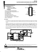
TPS5103 MULTIPLE MODE SYNCHRONOUS DC/DC CONTROLLER SLVS240A – SEPTEMBER 1999 – REVISED MAY 2001 functional block diagram SOFTSTART Softstart _ + FB PWM Comp. _ _ INV + LH OUT_u + Error Amp LL 1.185 V OUT_d OUTGND One Shot ON PWM/SKIP _ TRIP + CT RT OSC Disable _ VCC_SENSE + _ 1.185 V UVLO + VREF5 Comp GND VCC VREF _ STBY REF + 1.
TPS5103 MULTIPLE MODE SYNCHRONOUS DC/DC CONTROLLER SLVS240A – SEPTEMBER 1999 – REVISED MAY 2001 Terminal Functions TERMINAL NAME NO. I/O DESCRIPTION COMP 8 I Comparator input for voltage monitor CT 4 I/O External capacitor from CT to GND for adjusting the triangle oscillator and decreasing the current-limiting voltage FB 3 O Feedback output of error amp GND 6 INV 2 I LH 20 I/O Bootstrap. Connect a 1 µF, low-ESR capacitor from LH to LL. LL 18 I/O Bootstrap low.
TPS5103 MULTIPLE MODE SYNCHRONOUS DC/DC CONTROLLER SLVS240A – SEPTEMBER 1999 – REVISED MAY 2001 detailed description REF The reference voltage is used for the output voltage setting and the voltage protection(COMP). The tolerance is 1.5% typically. VREF5 An internal linear voltage regulator is used for the high-side driver bootstrap voltage. Since the input voltage range is from 4.5 V to 25 V, this voltage offers a fixed voltage for the bootstrap voltage so that the design for the bootstrap is much easier.
TPS5103 MULTIPLE MODE SYNCHRONOUS DC/DC CONTROLLER SLVS240A – SEPTEMBER 1999 – REVISED MAY 2001 detailed description (continued) softstart SOFTSTART sets the sequencing of the output for any possibility. The capacitor value for a start-up time can be calculated by the following equation: C = 2 x T (µF) Where C is the external capacitor value, and T is the required start-up time in (ms). standby The controller can be switched into the standby mode by grounding the STBY terminal.
TPS5103 MULTIPLE MODE SYNCHRONOUS DC/DC CONTROLLER SLVS240A – SEPTEMBER 1999 – REVISED MAY 2001 absolute maximum ratings over operating free-air temperature (unless otherwise noted)† Supply voltage, VCC (see Note 1) . . . . . . . . . . . . . . . . . . . . . . . . . . . . . . . . . . . . . . . . . . . . . . . . . . . –0.3 V to 27 V Input voltage, VI, INV, CT, RT, PWM/SKIP, SOFTSTART, COMP . . . . . . . . . . . . . . . . . . . . . . . . . . –0.3 V to 7 V Input voltage, VREG5V_IN . . . . . . . . . . . . . . .
TPS5103 MULTIPLE MODE SYNCHRONOUS DC/DC CONTROLLER SLVS240A – SEPTEMBER 1999 – REVISED MAY 2001 electrical characteristics over recommended operating free-air temperature range, VCC = 7 V (unless otherwise noted) reference voltage PARAMETER Vreff Reference voltage Regin† Regl† Line regulation Load regulation † Not a JEDEC symbol. TEST CONDITIONS TA = 25°C, Ivref = 50 µA Ivref = 50 µA VCC = 4.5 V to 25 V, I = 1 µA to 1 mA I = 50 µA MIN TYP MAX 1.167 1.185 1.203 1.155 1.215 UNIT V 0.
TPS5103 MULTIPLE MODE SYNCHRONOUS DC/DC CONTROLLER SLVS240A – SEPTEMBER 1999 – REVISED MAY 2001 electrical characteristics over recommended operating free-air temperature range, VCC = 7 V (unless otherwise noted) (continued) 5-V regulator PARAMETER TEST CONDITIONS VO Regin† Output voltage I = 10 mA Line regulation Regl† Load regulation VCC = 5.5 V to 25 V, I = 1 mA to 10 mA, IOS Short-circuit output current † Not a JEDEC symbol. MIN TYP 4.7 MAX UNIT 5.3 V I = 10 mA 20 mV VCC = 5.
TPS5103 MULTIPLE MODE SYNCHRONOUS DC/DC CONTROLLER SLVS240A – SEPTEMBER 1999 – REVISED MAY 2001 electrical characteristics over recommended operating free-air temperature range, VCC = 7 V (unless otherwise noted) (continued) softstart PARAMETER I(CTRL) VIT(high) Softstart current VIT(low) Threshold voltage (SKIP mode) TEST CONDITIONS MIN TYP MAX 1.9 2.5 3 3.9 UNIT µA V 2.6 output voltage monitor PARAMETER VIT TEST CONDITIONS Threshold voltage MIN TYP MAX UNIT 1.08 1.18 1.
TPS5103 MULTIPLE MODE SYNCHRONOUS DC/DC CONTROLLER SLVS240A – SEPTEMBER 1999 – REVISED MAY 2001 TYPICAL CHARACTERISTICS QUIESCENT CURRENT vs JUNCTION TEMPERATURE QUIESCENT CURRENT vs JUNCTION TEMPERATURE 700 50 45 600 VCC = 25 V 550 VCC = 7 V 500 VCC = 4.5 V 450 400 I CC– Quiescent Current – µ A I CC – Quiescent Current – µ A 650 VCC = 25 V 40 35 VCC = 7 V 30 25 VCC = 4.
TPS5103 MULTIPLE MODE SYNCHRONOUS DC/DC CONTROLLER SLVS240A – SEPTEMBER 1999 – REVISED MAY 2001 TYPICAL CHARACTERISTICS DRIVE OUTPUT VOLTAGE vs DRIVE SOURCE CURRENT DRIVE OUTPUT VOLTAGE vs DRIVE SOURCE CURRENT 4.5 6 TJ = 25°C VO(OUT_d)– Drive Output Voltage – V VO(OUT_d)– Drive Output Voltage – V TJ = 25°C 5 4 3 2 1 4 3.5 3 2.5 2 1.5 1 0.5 0 0 1 0.1 0.7 IS(OUT_sink) – Drive Source Current – A 1 0.7 IS(OUT_source) – Drive Source Current – A 0.
TPS5103 MULTIPLE MODE SYNCHRONOUS DC/DC CONTROLLER SLVS240A – SEPTEMBER 1999 – REVISED MAY 2001 TYPICAL CHARACTERISTICS ERROR AMPLIFIER INPUT OFFSET VOLTAGE vs JUNCTION TEMPERATURE ERROR AMPLIFIER OUTPUT VOLTAGE vs JUNCTION TEMPERATURE 2.5 VO – Error Amplifier Output Voltage – mV VIO – Error Amplifier Input Offset Voltage – mV 2.5 2 1.5 VCC = 4.5 V, VCC = 7 V, VCC = 25 V 1 0.5 2 1.5 1 0.5 0 –40 VCC = 4.
TPS5103 MULTIPLE MODE SYNCHRONOUS DC/DC CONTROLLER SLVS240A – SEPTEMBER 1999 – REVISED MAY 2001 TYPICAL CHARACTERISTICS VREF5 OUTPUT VOLTAGE vs SUPPLY VOLTAGE 2.5 5.2 VCC = 4.5 V, VCC = 7 V 2 VCC = 25 V 1.5 VCC = 25 V 1 VCC = 4.5 V VCC = 7 V 0.5 TJ = –40°C 5.1 VO – VREF5 Output Voltage – V VIH,VIL – Standby Switch Threshold Voltage – V STANDBY SWITCH THRESHOLD VOLTAGE vs JUNCTION TEMPERATURE 5 TJ = 125°C 4.9 TJ = 25°C 4.8 4.7 4.6 4.5 4.4 4.3 0 95 –25 25 TJ – Junction Temperature – °C –45 4.
TPS5103 MULTIPLE MODE SYNCHRONOUS DC/DC CONTROLLER SLVS240A – SEPTEMBER 1999 – REVISED MAY 2001 TYPICAL CHARACTERISTICS UVLO HYSTERESIS VOLTAGE vs JUNCTION TEMPERATURE UVLO THRESHOLD VOLTAGE vs JUNCTION TEMPERATURE 80 Vhys– UVLO Hysteresis Voltage – mV VTHL,VTLH – UVOL Threshold Voltage – V 4 3.95 VTLH 3.90 3.85 VTHL 3.80 3.75 70 60 50 40 30 20 10 0 3.70 –40 85 –20 25 TJ – Junction Temperature – °C –40 125 Figure 19 5 VSW HYSTERESIS VOLTAGE vs JUNCTION TEMPERATURE 200 4.
TPS5103 MULTIPLE MODE SYNCHRONOUS DC/DC CONTROLLER SLVS240A – SEPTEMBER 1999 – REVISED MAY 2001 TYPICAL CHARACTERISTICS SOFTSTART THRESHOLD VOLTAGE vs JUNCTION TEMPERATURE SOFTSTART CURRENT vs JUNCTION TEMPERATURE 4.5 VTLH – Softstart Threshold Voltage – V I CTRL – Softstart Current – µ A –2.45 –2.40 –2.35 VCC = 4.5 V VCC = 7 V –2.30 VCC = 25 V –2.25 4 3.5 3 2.5 VCC = 7 V, VCC = 25 V 2 1.5 1 0.5 0 –2.
TPS5103 MULTIPLE MODE SYNCHRONOUS DC/DC CONTROLLER SLVS240A – SEPTEMBER 1999 – REVISED MAY 2001 TYPICAL CHARACTERISTICS OSCILLATOR FREQUENCY vs JUNCTION TEMPERATURE OSCILLATOR OUTPUT VOLTAGE vs FREQUENCY 600 VOSCH,VOSCL– Oscillator Output Voltahe – V 1.6 f osc– Oscillator Frequency – kHz f = 500 kHz 500 VCC = 4.5 V, VCC = 7 V, VCC = 25 V 400 VCC = 4.5 V, VCC = 7 V, VCC = 25 V 300 200 f = 200 kHz 100 0 –40 85 –20 25 TJ – Junction Temperature – °C 125 1.4 VOSCH 1.2 1 0.8 0.6 VOSCL 0.4 0.
TPS5103 MULTIPLE MODE SYNCHRONOUS DC/DC CONTROLLER SLVS240A – SEPTEMBER 1999 – REVISED MAY 2001 TYPICAL CHARACTERISTICS MAXIMUM DUTY CYCLE vs JUNCTION TEMPERATURE SOFTSTART CAPACITANCE vs SOFTSTART TIME 100 104 f = 200 kHz C SS – Softstart Capacitance – pF 99.5 Maximum Duty Cycle – % 99 98.5 98 97.5 97 96.5 96 103 102 95.5 95 100 0.01 85 125 –20 25 TJ – Junction Temperature – °C –40 0.
TPS5103 MULTIPLE MODE SYNCHRONOUS DC/DC CONTROLLER SLVS240A – SEPTEMBER 1999 – REVISED MAY 2001 TYPICAL CHARACTERISTICS CURRENT PROTECTION SOURCE CURRENT vs INPUT VOLTAGE SKIP MODE I TRIP – Current Protection Source Current – µ A 4.6 TA = 125°C 4.5 4.4 TA = 25°C 4.3 4.2 TA = –40°C 4.1 4 4.
TPS5103 MULTIPLE MODE SYNCHRONOUS DC/DC CONTROLLER SLVS240A – SEPTEMBER 1999 – REVISED MAY 2001 APPLICATION INFORMATION overshoot of output rectangle wave The drivers in the TPS5103 controller are fast and can produce high transients on VCC or the junction of Q1 and Q2 (shown below). Care must be taken to insure that these transients do not exceed the absolute maximum rating for the device or associated external component.
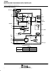
TPS5103 MULTIPLE MODE SYNCHRONOUS DC/DC CONTROLLER SLVS240A – SEPTEMBER 1999 – REVISED MAY 2001 APPLICATION INFORMATION Resistor (Rg) is moved from the gate of the top FET and placed in series with LL. This allows for a smaller Schottky diode (DX) to be used. OUT_u Q1 Rg LL DX Q2 Figure 38. High-Current Schottky Diode Removed application for general power The design shown in this data sheet is a reference design for a general power supply application.
TPS5103 MULTIPLE MODE SYNCHRONOUS DC/DC CONTROLLER SLVS240A – SEPTEMBER 1999 – REVISED MAY 2001 APPLICATION INFORMATION output voltage setpoint calculation The output voltage is set by the reference voltage and the voltage divider. In the TPS5102, the reference voltage is 1.185 V, and the divider is composed of two resistors in the EVM design that are R4 and R5, or R14 and R15. The equation for the setpoint is shown below.
TPS5103 MULTIPLE MODE SYNCHRONOUS DC/DC CONTROLLER SLVS240A – SEPTEMBER 1999 – REVISED MAY 2001 APPLICATION INFORMATION switching frequency With hysteretic control, the switching frequency is a function of the following: D D D D D D D D D D input voltage output voltage hysteresis window delay of the hysteresis comparator and the driver output inductance resistance in the output inductor output capacitance ESR and ESL in the output capacitor output current turnon resistance of the high-side and the low-si
TPS5103 MULTIPLE MODE SYNCHRONOUS DC/DC CONTROLLER SLVS240A – SEPTEMBER 1999 – REVISED MAY 2001 APPLICATION INFORMATION output capacitor RMS current Where IO(rms) is the maximum RMS current in the output capacitor (A), and ∆I is the peak-to-peak inductor ripple current (A). Example: ∆I = 2 A, so IO(rms) = 0.
TPS5103 MULTIPLE MODE SYNCHRONOUS DC/DC CONTROLLER SLVS240A – SEPTEMBER 1999 – REVISED MAY 2001 APPLICATION INFORMATION loop-gain compensation Voltage mode control is used in this controller for the output voltage regulation. To achieve fast, stabilized control, two parts are discussed in this section: the power stage small signal modeling and the compensation circuit design. For the buck converter, the small-signal modeling circuit is shown in Figure 41.
TPS5103 MULTIPLE MODE SYNCHRONOUS DC/DC CONTROLLER SLVS240A – SEPTEMBER 1999 – REVISED MAY 2001 APPLICATION INFORMATION loop-gain compensation (continued) R1 R2 R4 C3 C1 _ R3 C2 To PWM + Vref Figure 43. Typical Compensation Circuit This circuit is composed of one integrator, two poles, and two zeros.
TPS5103 MULTIPLE MODE SYNCHRONOUS DC/DC CONTROLLER SLVS240A – SEPTEMBER 1999 – REVISED MAY 2001 APPLICATION INFORMATION loop-gain compensation (continued) There is one pole, one zero, and one integrator. Zero 1 + 2pC3R4 Pole 1 + 2pC2R4 Integrator 1 + 2pƒC3R2 The loop-gain concept is used to design a stable and fast feedback control. The loop-gain equation is derived by the control-to-output transfer function times the compensation. The equation is shown below.
TPS5103 MULTIPLE MODE SYNCHRONOUS DC/DC CONTROLLER SLVS240A – SEPTEMBER 1999 – REVISED MAY 2001 APPLICATION INFORMATION synchronization (continued) 740 mV CT TPS5103 740 mV RT Figure 46. Triangle-Wave Synchronization D Square-wave synchronization It can be seen that RT and CT are removed from the circuit. Therefore, two components are saved. This method is good for the synchronization between two controllers.
TPS5103 MULTIPLE MODE SYNCHRONOUS DC/DC CONTROLLER SLVS240A – SEPTEMBER 1999 – REVISED MAY 2001 APPLICATION INFORMATION layout guidelines (continued) D D D D D D D When configuring the high-side driver as a floating driver, the connection from LL to the power FETs should be as short and as wide as possible. When configuring the high-side driver as a floating driver, the bootstrap capacitor (connected from LH to LL) should be placed close to the TPS5103.
TPS5103 MULTIPLE MODE SYNCHRONOUS DC/DC CONTROLLER SLVS240A – SEPTEMBER 1999 – REVISED MAY 2001 APPLICATION INFORMATION EFFICIENCY vs OUTPUT CURRENT EFFICIENCY vs OUTPUT CURRENT 95 95 1.8-V Output Efficiency 1.8-V Output Efficiency 90 90 PWM Mode 85 Efficiency – % Efficiency – % 85 80 75 PWM Mode 80 75 SKIP Mode SKIP Mode 70 70 65 65 60 60 0 0.5 3.5 1 1.5 2 2.5 3 IO – Output Current – A 0 4 0.1 Figure 48 0.4 0.2 0.3 IO – Output Current – A 0.
TPS5103 MULTIPLE MODE SYNCHRONOUS DC/DC CONTROLLER SLVS240A – SEPTEMBER 1999 – REVISED MAY 2001 APPLICATION INFORMATION EFFICIENCY vs OUTPUT CURRENT OUTPUT/VOLTAGE OUTPUT VOLTAGE 95 1.8-V Output Diode Type Efficiency 90 Efficiency – % 85 80 75 70 65 60 0 0.5 1 1.5 2 2.5 3 IO – Output Current – A 3.
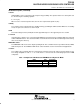
TPS5103 MULTIPLE MODE SYNCHRONOUS DC/DC CONTROLLER SLVS240A – SEPTEMBER 1999 – REVISED MAY 2001 APPLICATION INFORMATION Table 3.
TPS5103 MULTIPLE MODE SYNCHRONOUS DC/DC CONTROLLER SLVS240A – SEPTEMBER 1999 – REVISED MAY 2001 APPLICATION INFORMATION Figure 56. Top Layer . Figure 57.
TPS5103 MULTIPLE MODE SYNCHRONOUS DC/DC CONTROLLER SLVS240A – SEPTEMBER 1999 – REVISED MAY 2001 APPLICATION INFORMATION Figure 58. Top Assembly – Power Supply Load 0–4A + 5-V, 5-A Supply – + NOTE: All wire pairs should be twisted. Figure 59.
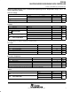
TPS5103 MULTIPLE MODE SYNCHRONOUS DC/DC CONTROLLER SLVS240A – SEPTEMBER 1999 – REVISED MAY 2001 APPLICATION INFORMATION Table 4. Test Specifications PARAMETER CONDITIONS MIN Input voltage range, VI TYP 5 Output voltage range, VO Output current range, IO Output current limit Output ripple Operating frequency, f Efficiency VI = 5 – 25 V, IO = 0 – 4 A VI = 5 – 10 V 1.7 VI = 5 V VI = 5 V, IO = 4 A 4.3 IO = 4 A VI = 5 V, VO = 1.8 V, IO = 4 A 150 1.8 0 MAX UNITS 25 V 1.
TPS5103 MULTIPLE MODE SYNCHRONOUS DC/DC CONTROLLER SLVS240A – SEPTEMBER 1999 – REVISED MAY 2001 APPLICATION INFORMATION High-current applications are described in Table 8. The values are recommendations based on actual test circuits. Many variations are possible based on the requirements of the user. Performance of the circuit is dependent upon the layout rather than on the specific components, if the device parameters are not exceeded.
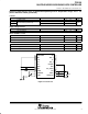
TPS5103 MULTIPLE MODE SYNCHRONOUS DC/DC CONTROLLER SLVS240A – SEPTEMBER 1999 – REVISED MAY 2001 MECHANICAL DATA DB (R-PDSO-G**) PLASTIC SMALL-OUTLINE PACKAGE 28 PINS SHOWN 0,38 0,22 0,65 28 0,15 M 15 0,15 NOM 5,60 5,00 8,20 7,40 Gage Plane 1 14 0,25 A 0°– 8° 1,03 0,63 Seating Plane 2,00 MAX 0,10 0,05 MIN PINS ** 8 14 16 20 24 28 30 38 A MAX 3,30 6,50 6,50 7,50 8,50 10,50 10,50 12,90 A MIN 2,70 5,90 5,90 6,90 7,90 9,90 9,90 12,30 DIM 4040065 / C 10/95 NOTES: A.
PACKAGE OPTION ADDENDUM www.ti.
PACKAGE MATERIALS INFORMATION www.ti.com 11-Mar-2008 TAPE AND REEL INFORMATION *All dimensions are nominal Device TPS5103IDBR Package Package Pins Type Drawing SSOP DB 20 SPQ Reel Reel Diameter Width (mm) W1 (mm) 2000 330.0 16.4 Pack Materials-Page 1 A0 (mm) B0 (mm) K0 (mm) P1 (mm) W Pin1 (mm) Quadrant 8.2 7.5 2.5 12.0 16.
PACKAGE MATERIALS INFORMATION www.ti.com 11-Mar-2008 *All dimensions are nominal Device Package Type Package Drawing Pins SPQ Length (mm) Width (mm) Height (mm) TPS5103IDBR SSOP DB 20 2000 346.0 346.0 33.
IMPORTANT NOTICE Texas Instruments Incorporated and its subsidiaries (TI) reserve the right to make corrections, modifications, enhancements, improvements, and other changes to its products and services at any time and to discontinue any product or service without notice. Customers should obtain the latest relevant information before placing orders and should verify that such information is current and complete.