
Datasheet

1
2
3
4
12
11
10
9
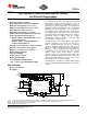
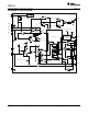
SW
DH
DL
V5
VREF
REFIN
GSNS
VSNS
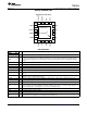
TPS51219RTE
5 6 7 8
PGND
GND
TRIP
COMP
16 15 14 13
BST
EN
MODE
PGOOD
PwrPd
VSNS
GSNS
PGOOD
V5IN
EN
V
OUT
V
IN
UDG-11006
TPS51219
www.ti.com
SLUSAG1B –MARCH 2011– REVISED OCTOBER 2011
High Performance, Single-Synchronous Step-Down Controller
with Differential Voltage Feedback
1
FEATURES
DESCRIPTION
The TPS51219 is a small-sized single buck controller
23
• Differential Voltage Feedback
with adaptive on-time control. It provides a choice of
• DC Compensation for Accurate Regulation
control modes (D-CAP™ or D-CAP2™) to meet a
• Wide Input Voltage Range: 3 V to 28 V
wide range of system requirements. It is designed for
tight DC regulation requirements such as the VCCIO
• Output Voltage Range: 0.5 V to 2.0 V with
application for Intel
®
notebooks. The performance
Fixed Options of 1.05 V and 1.00 V
and flexibility of the TPS51219 makes it suitable for
• Wide Output Load Range: 0 A to 20 A+
low output voltage, high current, PC system power
• Adaptive On-Time Modulation with Selectable
rails and similar point-of-load (POL) power supplies.
Control Architecture and Frequency
Differential voltage feedback and the voltage
compensation function combine to provide high
– D-CAP™ Mode at 300 kHz/400 kHz for Fast
precision power to load devices.
Transient Response
A small package, fixed voltage options and minimal
– D-CAP2™ Mode at 500 kHz/670 kHz for
external component count saves cost and space,
Ceramic Output Capacitor
while a dedicated EN pin and pre-set frequency
• 4700 ppm/°C, Low-Side R
DS(on)
Current Sensing
selections minimize design effort. The skip-mode at
• R
SENSE
Accurate Current Sense Option
light load condition, strong gate drivers, and low-side
FET R
DS(on)
current sensing provides high efficiency
• Internal, 1-ms Voltage Servo Softstart
operation over a broad load range. The external
• Built-In Output Discharge
resistor current sense option enables accurate
• Power Good Output
current sensing. The conversion input voltage (the
high-side FET drain voltage) ranges from 3 V to 28 V
• Integrated Boost Switch
and output voltage ranges from 0.5 V to 2.0 V. The
• Built-In OVP/UVP/OCP
device requires an external 5-V supply.
• Thermal Shutdown (Non-latched)
The TPS51219 is available in a 16-pin, QFN package
• 3 mm × 3 mm, 16-Pin, QFN (RTE) Package
and is specified for ambient temperature from -40°C
to 85°C.
APPLICATIONS
• Notebook Computers
• I/O Supplies
1
Please be aware that an important notice concerning availability, standard warranty, and use in critical applications of Texas
Instruments semiconductor products and disclaimers thereto appears at the end of this data sheet.
2D-CAP, D-CAP2 are trademarks of Texas Instruments.
3Intel is a registered trademark of Intel.
PRODUCTION DATA information is current as of publication date.
Copyright © 2011, Texas Instruments Incorporated
Products conform to specifications per the terms of the Texas
Instruments standard warranty. Production processing does not
necessarily include testing of all parameters.