
Datasheet


SLUS571 − SEPTEMBER 2003
5
www.ti.com
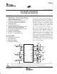
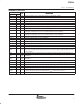
TERMINAL FUNCTIONS
TERMINAL
I/O
DESCRIPTION
NAME NO.
I/O
DESCRIPTION
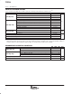
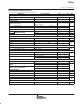
CT 5 I/O External capacitor from CT to GND adjusts frequency of the triangle oscillator.
FB1 2 O Feedback output of SBRC−Channel 1 error amplifier.
FB2 14 O Feedback output of SBRC−Channel 2 error amplifier.
GND 7 − Signal GND.
INV1 1 I Inverting inputs of Channel 1 error amplifier and OVP1/UVP1 comparator.
INV2 15 I Inverting inputs of Channel 2 error amplifier and OVP2/UVP2 comparator.
LH1 30 I/O Bootstrap capacitor connection for Channel 1 high-side gate driver.
LH2 16 I/O Bootstrap capacitor connection for Channel 2 high-side gate driver.
LL1 28 I/O
CH1 high-side gate driving return. Connect this pin to the junction of the high-side and low-side MOSFETs for
floating drive configuration. This pin is also an input terminal for current comparator.
LL2 18 I/O
CH2 high-side gate driving return. Connect this pin to the junction of the high-side and low-side MOSFETs for
floating drive configuration. This pin is also an input terminal for current comparator.
NC 4,6,12 − No connection.
OUT1_D 27 O Gate drive output for Channel 1 low-side MOSFETs.
OUT2_D 19 O Gate drive output for Channel 2 low-side MOSFETs.
OUT1_U 29 O Gate drive output for Channel 1 high-side MOSFETs.
OUT2_U 17 O Gate drive output for Channel 2 high-side MOSFETs.
OUTGND1 26 − Ground for Channel 1 MOSFET drivers.
OUTGND2 20 − Ground for Channel 2 MOSFET drivers.
REF 8 O
0.85-V reference voltage output. This 0.85-V reference voltage is used to set the output voltage and the refer-
ence for the overvoltage and undervoltage protections. This reference voltage is dropped down from the inter-
nal 5-V regulator.
SCP 11 I/O Fault latch timer pin. An external capacitor connected between SCP and GND sets SCP enable time up.
SS1 3 I/O
Soft start control for Channel 1. Connect an external capacitor between this pin and GND to specify SOFT-
START time.
SS2 13 I/O
Soft start control for Channel 2. Connect an external capacitor between this pin and GND to specify SOFT-
START time.
STBY1 9 I Standby control input for Channel 1. It can be switched into standby mode by grounding the STBY1 pin.
STBY2 10 I Standby control input for Channel 2. It can be switched into standby mode by grounding the STBY2 pin.
TRIP1 25 I External resistor connection for Channel 1 output current protection control.
TRIP2 23 I External resistor connection for Channel 2 output current protection control.
VCC 24 I Supply voltage input
VLSD 21 I
Supply voltage input for low side driver. Typically connected to VREF5 with R-C filter when V
VCC
is between
6.5V and 15V and connected to VCC with filter when V
VCC
is between 4.5 V and 5.5 V.
VREF5 22 O 5V linear regulator output. When V
VCC
is between 4.5V and 5.5V should be connected to VCC.