
Datasheet


SLUS571 − SEPTEMBER 2003
8
www.ti.com
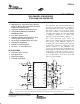
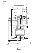
FUNCTIONAL DESCRIPTION
OVER CURRENT PROTECTION (OCP)
Over current protection (OCP) is achieved by comparing the drain-to-source voltage of the high-side and
low-side MOSFET to a set-point voltage, which is defined by both the internal current source, I
TRIP
, and the
external resistor connected between the VCC and TRIP pins. I
TRIP
has a typical value of 13 µA at 25°C. When
the low-side MOSFET’s drain-to-source voltage exceeds the set-point voltage during low-side conduction, the
high-side current comparator becomes active, and the low-side on pulse is extended until this voltage comes
back below the threshold. If the set-point voltage is exceeded during high-side conduction in the following cycle,
the current limit circuit terminates the high-side driver pulse. Together this action has the effect of decreasing
the output voltage until the under voltage protection circuit is activated to latch both the high-side and low-side
drivers OFF. In the TPS5124, trip current (I
TRIP
) has a temperature coefficient of 3400 ppm/_C in order to
compensate for temperature drift of the MOSFET on-resistance.
OVER VOLTAGE PROTECTION (OVP)
For over voltage protection (OVP), the TPS5124 monitors the INV pin voltage. When the INV pin voltage is
higher than 0.95 V (0.85 V +12%), the OVP comparator output goes low and the SCP timer starts to charge an
external capacitor connected to SCP pin. After a set time, the SCP circuit latches the high-side MOSFET driver
to OFF state and low-side MOSFET drivers to ON state. The timer source current for the OVP latch is 8 µA(typ.),
and the time−up voltage is 1.185 V (typ.). The OVP timer is designed to be five times faster than the under
voltage protection timer described below.
UNDER VOLTAGE PROTECTION (UVP)
For under voltage protection (UVP), the TPS5124 monitors the INV pin voltage. When the INV pin voltage is
lower than 0.66 V (0.85 V – 22%), the UVP comparator output goes low, and the SCP timer starts to charge the
external capacitor connected to SCP pin. Also, when the current comparator triggers the OCP, the UVP
comparator detects the under voltage output and starts the SCP capacitor charge, too. After a set time, the SCP
circuit latches both of the MOSFET drivers to the OFF state. The timer latch source current for UVP is 1.6 µA
(typ.), and the time-up voltage is also 1.185 V (typ.).
SCP (TIMER)
When an OVP or UVP comparator output goes low, the SCP circuit starts to charge the SCP capacitor. If the
SCP pin voltage goes beyond a constant level, the TPS5124 latches the MOSFET drivers. At this time, the state
of MOSFET is different depending on the OVP alert and the UVP alert. The enable time used to latch the
MOSFET drivers is decided by the value of the SCP capacitor. The charging constant current value depends
on whether it is an OVP alert or a UVP alert as shown in the following equation:
I
SCP(ovp)
+ I
SCP(uvp)
5
SOFT START
Soft-start ramp up of the SBRC is controlled by the SSx pin voltage. After the STBY pin is raised to a HIGH level,
an internal current source charges up an external capacitor connected between the SSx and GND pins. The
soft-start time is easily calculated by the supply current and the capacitance value.
(1)