User’s Guide User’s Guide 1
EVM IMPORTANT NOTICE Texas Instruments (TI) provides the enclosed product(s) under the following conditions: This evaluation kit being sold by TI is intended for use for ENGINEERING DEVELOPMENT OR EVALUATION PURPOSES ONLY and is not considered by TI to be fit for commercial use.
DYNAMIC WARNINGS AND RESTRICTIONS It is important to operate this EVM within the input voltage range of 0 Vdc to100 Vdc. Exceeding the specified input range may cause unexpected operation and/or irreversible damage to the EVM. If there are questions concerning the input range, please contact a TI field representative prior to connecting the input power. Applying loads outside of the specified output range may result in unintended operation and/or possible permanent damage to the EVM.
SLUU182 − March 2004 High-Performance Dual Synchronous Buck Conversion Using the TPS5124 Systems Power Contents 1 Introduction . . . . . . . . . . . . . . . . . . . . . . . . . . . . . . . . . . . . . . . . . . . . . . . . . . . . . . . . . . . . . . . . . . . . . . . . . 4 2 Features . . . . . . . . . . . . . . . . . . . . . . . . . . . . . . . . . . . . . . . . . . . . . . . . . . . . . . . . . . . . . . . . . . . . . . . . . . . . 5 3 Schematic . . . . . . . . . . . . . . . . . . . . . . . . . . .
SLUU182 − March 2004 2 Features This EVM is designed to operate from 12-V bus voltage. It generates two outputs, 3.3 V at 15 A and 1.5 V at 10 A. Table 1. TPS5124EVM−001 Performance Summary PARAMETER TEST CONDITIONS MIN Input voltage range TYP 6.5 Operating frequency Input ripple voltage (RMS) VIN = 12 V, IOUT1 = 15 A, IOUT2 = 10 A 12.0 MAX 15.0 UNITS V 300 kHz 92 mV Channel 1 Output current range 6.5 V ≤ VIN ≤ 15 V Line regulation 6.
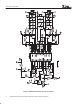
+ + SLUU182 − March 2004 Figure 1.
SLUU182 − March 2004 4 Design Procedure 4.1 Frequency Setting Many factors influence frequency selection. Higher switching frequency leads to smaller output inductor and capacitor, reducing the size of the converter. However, higher switching frequencies increase switching losses, and lower the converter’s efficiency. A frequency of 300 kHz is chosen for this design for reasonable efficiency and size. Capacitor C16, which is connected from CT (pin 5) to ground, programs the oscillator frequency.
SLUU182 − March 2004 where • VOUT2 is the allowed overshoot voltage • VOUT1 is the nominal operating voltage For 6% overshoot, the required capacitance is about 370 µF. Four 100-µF, 6.3-V ceramic capacitors are used. Their ESR value is 2.0 mΩ each. 4.4 Input Capacitors Due to the out of phase operation, the input current ripple is partially cancelled. The total RMS current in the input capacitor is calculated as follows.
SLUU182 − March 2004 4.4.1 Case One: D1, D2 < 0.5. The ripple current through the input capacitor is shown in Figure 2 and can be calculated using equation (6). I incapRMS :+ Ǹ 1 T ȱŕ ȧ Ȳ D1@T ǒIOUT1 * IAVGǓ 2 dt ) ǒI AVGǓ 2 dt ) D1@T 0 ǸD1 I incapRMS :+ ŕ T 2 ǒIOUT1Ǔ 2 ) D2 ǒIOUT2Ǔ 2 ŕ T)D2@T 2 T 2 ǒIOUT2 * IAVGǓ * ǒI AVGǓ 2 dt ) ŕ T T)D2@T 2 ǒIAVGǓ ȳ (5) ȧ ȴ 2 dt 2 (6) where: IAVG is the average input current. I AVG + I OUT1 4.4.
SLUU182 − March 2004 4.5 Compensation Design The following compensation loop design uses Channel 1 as example, but a design for Channel 2 follows the same rules. TPS5124 uses voltage-mode control method. A Type III compensation network, formed by R1, R2, R4, C14, C12, and C23, is used to guarantee the stability. The L-C frequency of the power stage is around 5.4 kHz and the ESR zero is at 790 KHz due to the low ESR of the ceramic capacitors.
SLUU182 − March 2004 Figure 4 shows the closed loop gain and phase. For Channel 1, the overall crossover frequency is approximately 30 kHz and the phase margin is 58°. For Channel 2, the crossover frequency is approximately 23 kHz and phase margin is 55°. 4.6 Current Limiting The current limit in TPS5124 is set using an internal current source and an external resistor (R13 and R14).
SLUU182 − March 2004 4.7 Timer Latch The TPS5124 includes fault latch function with a user adjustable timer to latch the MOSFET drivers in case of a fault condition. When either the OVP or UVP comparator detect a fault condition, the timer starts to charge C18, the external capacitor connected to the SCP pin. The circuit is designed so that for any value of C18, the undervoltage latch time tUVPL is about five times larger than the overvoltage latch time tOVPL.
SLUU182 − March 2004 4.7.4 Disabling the Protection Function If it is necessary to disable the protection functions of the TPS5124 for troubleshooting or other purposes, the OCP, OVP and UVP circuits may be disabled. 4.7.4.1 Disabling Overcurrent Protection (OCP) Remove the current limit resistors R13 and R14 to disable the current limit function. 4.7.4.2 Disabling Overvoltage Protection or Undervoltate Protection (OVP, UVP) Grounding the SCP terminal can disable OVP and UVP.
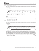
SLUU182 − March 2004 5 Test Results 5.1 Efficiency Curves The efficiency was tested under three different operation conditions. OVERALL EFFICIENCY vs OUTPUT CURRENT VOUT2 (1.5 V) Enabled Only OVERALL EFFICIENCY vs OUTPUT CURRENT VOUT1 (3.3 V) Enabled Only 96 92 VIN = 6.5 V VIN = 6.5 V 90 94 Percent Efficiency − % Percent Efficiency − % 95 VIN = 12 V 93 92 91 88 86 VIN = 12 V 84 82 VIN = 15 V 80 90 78 VIN = 15 V 76 89 0 3 6 9 IOUT − Output Current − A 12 15 0 Figure 6.
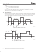
SLUU182 − March 2004 OVERALL EFFICIENCY vs OUTPUT POWER Both Channels Enabled 96 Percent Efficiency − % 94 VIN = 6.5 V 92 90 VIN = 15 V 88 VIN = 12 V 86 0 0.2 0.4 0.6 0.8 Output Power Over the Full Power 1.0 Figure 8. 5.2 Typical Operating Waveform Typical operating waveforms taken at VIN =12 V, IOUT1 = 15 A and IOUT2=10 A is shown in Figure 9. 5.3 Start-Up Waveform Figure 10 shows the start-up waveform taken at VIN =12 V, IOUT1 = 15 A and IOUT2=10 A. The rising time is 2.85 ms for VOUT1 and 2.
SLUU182 − March 2004 5.4 Output Ripple Voltage and Load Transient The output ripple is about 20 mVP−P at 15 A on Channel 1 (3.3 V) output and 15 mVP−P at 10 A on Channel 2 output as shown in Figure 11. Figure 12 shows the load transient response. For Channel 1 (3.3 V), when the load steps from 0 A to 8.5 A, the overshoot and undershoot voltages are about 150 mV. For Channel 2 (1.5 V), when the load steps from 0 A to 7.
SLUU182 − March 2004 6 Layout Guidelines Proper design and layout is crucial to the performance of the power supply. Here are some suggestions to the layout of TPS5124 design. 6.1 6.2 6.3 6.4 • A four−layer PCB design is recommended for designs using the TPS5124. Use at least one layer dedicated to the PWRGND plane. • All sensitive analog components such as INV, REF, CT, GND, SCP and SOFTSTART should be reference to ANAGND.
SLUU182 − March 2004 • 6.5 7 LH and LL should not be routed near the control pin area (e.g. INV, FB, REF, etc.). Output voltage • The output voltage sensing trace should be isolated by either ground plane. • The output voltage sensing trace should not be placed under the inductors on the same layer. • The feedback components should be isolated from output components, such as, MOSFETs, inductors, and output capacitors. Otherwise the feedback signal line is susceptible to output noise.
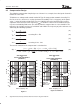
SLUU182 − March 2004 Figure 15. Top Side Figure 16.
SLUU182 − March 2004 Figure 17. Internal 2 Figure 18.
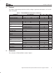
SLUU182 − March 2004 8 List of Materials Table 2. List of Materials REFERENCE DESIGNATOR QTY DESCRIPTION SIZE MFR PART NUMBER Std Std GRM32ER61A106KC01L Std C1,C2, C3 C12, C22 C13 C14, C20 C7, C15, C18, C19, C32, C16 C21, C23 C24, C25, C26, C27, C28, C29, C30, C31 3 2 1 2 Capacitor, ceramic, 2.2 µF, 50 V, X7R, 10% Capacitor, ceramic, 5600 pF, 50 V, X7R, 10% Capacitor, ceramic, 10 µF, 10 V, X5R, 10% Capacitor, ceramic, 0.
IMPORTANT NOTICE Texas Instruments Incorporated and its subsidiaries (TI) reserve the right to make corrections, modifications, enhancements, improvements, and other changes to its products and services at any time and to discontinue any product or service without notice. Customers should obtain the latest relevant information before placing orders and should verify that such information is current and complete.