
Datasheet

Introduction
www.ti.com
1 Introduction
1.1 Background
The TPS54020 dc/dc converter is designed to provide up to 10-A output current. The TPS54020
implements split-input power rails with separate input voltage inputs for the power stage and control
circuitry. The power stage input (PVIN) is rated for 1.6 V to 17 V whereas the control input (V
IN
) is rated for
4.5 V to 17 V. This EVM provides connections for both inputs but is designed and tested using the PVIN
connected to V
IN
. Rated input voltage and output current range for the EVM are given in Table 1. This
EVM is designed to demonstrate the small printed-circuit-board areas that may be achieved when
designing with the TPS54020 regulator. The switching frequency is externally set by a resistor at a
nominal 500 kHz. The high-side and low-side MOSFETs are incorporated inside the TPS54020 package
along with the gate-drive circuitry. The low drain-to-source ON resistance of the MOSFET allows the
TPS54020 to achieve high efficiencies and helps keep the junction temperature low at high output
currents. The compensation components are external to the integrated circuit (IC), and an external divider
allows for an adjustable output voltage. Additionally, the TPS54020 provides adjustable slow start and
undervoltage lockout inputs. The absolute maximum input voltage is 20 V for the EVM, but the
recommended maximum input voltage of 17 V should not be exceeded.
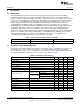
Table 1. Input Voltage and Output Current Summary
EVM Input Voltage Range Output Current Range
TPS54020EVM-082 VIN = 8 V to 17 V (V
IN
start voltage = 7.5 V) 0 A to 10 A
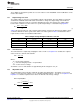
1.2 Performance Specification Summary
A summary of the EVM performance specifications is provided in Table 2. Specifications are given for an
input voltage of V
IN
= 12 V and an output voltage of 1.8 V, unless otherwise specified. This EVM is
designed and tested for V
IN
= 8 V to 17 V with the V
IN
and PVIN pins connect together with the jumper J2.
The ambient temperature is 25°C for all measurements, unless otherwise noted.
Table 2. Performance Specifications
Specification Test Conditions MIN TYP MAX UNIT
V
IN
voltage range (PV
IN
= V
IN
) 8 12 17 V
V
IN
start voltage 7.5 V
V
IN
stop voltage 7.1 V
Output voltage set point 1.8 V
Output current range V
IN
= 8 V to 17 V 0 10 A
Line regulation I
O
= 5 A, V
IN
= 8 V to 17 V ±0.3%
Load regulation V
IN
= 12 V, I
O
= 0 A to 10 A ±0.5%
Voltage change –150 mV
I
O
= 2.5 A to 47.5 A
Recovery time 200 µS
Load transient response
Voltage change 150 mV
I
O
= 47.5 A to 2.5 A
Recovery time 200 µS
Loop bandwidth V
IN
= 12 V, I
O
= 1.9 A 30 kHz
Phase margin V
IN
= 12 V , I
O
= 1.9 A 60 Degrees
Input ripple voltage I
O
= 10 A 300 mVpp
Output ripple voltage I
O
= 6 A 18 mVpp
Output rise time 26 mS
Operating frequency 500 kHz
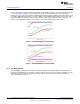
Peak efficiency TPS54020EVM-082, V
IN
= 12 V, I
O
= 5 A 89 %
2
TPS54020EVM-082 Evaluation Module (PWR082) SLVU777–September 2012
Submit Documentation Feedback
Copyright © 2012, Texas Instruments Incorporated