
Datasheet
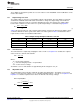
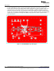

Time = 200 ms/div
V = 100 mV/div
OUT
AC coupled
I = 2.5 A /div
OUT
2.5 A to 7.5 A switching
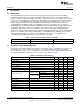
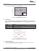
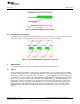
1.8
1.805
1.81
1.815
1.82
1.825
1.83
1.835
1.84
5 6 7 8 9 10 11 12 13 14 15 16 17
Input Voltage (V)
Output Voltage (V)
V
OUT
= 0.1 A
V
OUT
= 1 A
V
OUT
= 5 A
V
OUT
= 1 0 A
Temp = 25°C
G008
Test Setup and Results
www.ti.com
2.4 Output Voltage Line Regulation
Figure 3 shows the line regulation for the TPS54020EVM-082.
Figure 3. TPS54020EVM-082 Line Regulation
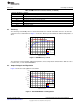
2.5 Load Transient
Figure 4 shows the EVM response to load transients. The current step is from 0 A to 4.7 A with an input
voltage of 5 V. The transient was applied by switching in a real resistor load. The current step slew rate is
approximately 50 A/μs. Total peak-to-peak voltage variation is as shown, including ripple and noise on the
output.
Parameter Description
Bottom Trace Output current switching between 2.5 A and 7.5 A, 2.5 A/div
Top trace Output voltage, AC coupled, at 100 mV/div
Time Scale 200 µs/div
Conditions Input voltage = 12 V, temperature = 25°C
Figure 4. TPS54020EVM-082 Transient Response
2.6 Control Loop Response
Figure 5 shows the EVM control loop response characteristics. Gain and phase plots are shown for V
IN
voltage of 12 V and a constant resistance load current of 5 A.
6
TPS54020EVM-082 Evaluation Module (PWR082) SLVU777–September 2012
Submit Documentation Feedback
Copyright © 2012, Texas Instruments Incorporated