
Datasheet
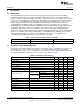
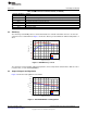
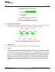

Time = 20 ms/div
I = 5 A/div
OUT
V = 500 mV/div
OUT
PH node = 10 V/div
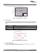
Time = 5 ms/div
V = 5 V/div
IN
V = 500 mV/div with
OUT
EN = 2 V/div
PH node = 10 V/div
1 V pre-bias
www.ti.com
Board Layout
Figure 10. TPS54020EVM-082 Pre-Bias Startup
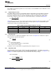
2.11 Hiccup Mode Current Limit
The EVM features hiccup mode current limit. When an overcurrent event occurs, the device shuts down
and restarts. Figure 11 shows the hiccup restart sequence in an over current condition.
Figure 11. TPS54020EVM-082 Hiccup Mode Current Limit
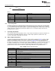
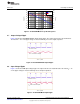
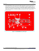
3 Board Layout
This section provides a description of the EVM board layout and layer illustrations.
3.1 Layout
The board layout for the EVM is shown in Figure 12 through Figure 17. The top-side layer of the EVM is
laid out in a manner typical of a user application. All 4 layers (top, bottom, and 2 internal) are 2-oz copper.
The top layer contains the main power traces for PVIN, V
IN
, V
OUT
and VPHASE. Also on the top layer are
connections for several analog pins of the TPS54020 and a large area filled with PGND. The two internal
layers are the same and contain mostly power planes, including PGND, V
OUT
, PVIN and VPHASE. The
bottom layer contains the remainder of the analog circuit connections, plus power planes similar to the
internal layers. The top-side power and ground planes are connected to the bottom and internal power
and ground planes with multiple vias placed around the board including several vias directly under the
TPS54020 device to provide a thermal path from the top-side power planes to the other layer power
planes.
9
SLVU777–September 2012 TPS54020EVM-082 Evaluation Module (PWR082)
Submit Documentation Feedback
Copyright © 2012, Texas Instruments Incorporated