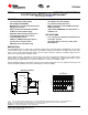
TPS54060A www.ti.com SLVSB57B – MARCH 2012 – REVISED SEPTEMBER 2013 0.5A, 60V Step Down DC/DC Converter with Eco-mode™ Check for Samples: TPS54060A FEATURES 1 • • • 23 • • • • • • • 3.5V to 60V Input Voltage Range 200-mΩ High-Side MOSFET High Efficiency at Light Loads with a Pulse Skipping Eco-mode™ Tighter Enable Threshold than TPS54060 for More Accurate UVLO Voltage Adjustable UVLO Voltage and Hysteresis 116μA Operating Quiescent Current 1.3μA Shutdown Current 100kHz to 2.
TPS54060A SLVSB57B – MARCH 2012 – REVISED SEPTEMBER 2013 www.ti.com These devices have limited built-in ESD protection. The leads should be shorted together or the device placed in conductive foam during storage or handling to prevent electrostatic damage to the MOS gates.
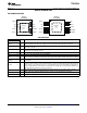
TPS54060A www.ti.com SLVSB57B – MARCH 2012 – REVISED SEPTEMBER 2013 THERMAL INFORMATION TPS54060A THERMAL METRIC (1) (2) DGQ (10 PINS) θJA Junction-to-ambient thermal resistance (standard board) 62.5 40 ψJT Junction-to-top characterization parameter 1.7 0.6 ψJB Junction-to-board characterization parameter 20.1 7.5 θJCtop Junction-to-case(top) thermal resistance 83 65 θJCbot Junction-to-case(bottom) thermal resistance 21 7.
TPS54060A SLVSB57B – MARCH 2012 – REVISED SEPTEMBER 2013 www.ti.com ELECTRICAL CHARACTERISTICS (continued) TJ = –40°C to 150°C, VIN = 3.5 to 60V (unless otherwise noted) PARAMETER TEST CONDITIONS MIN TYP MAX UNIT 0.6 0.
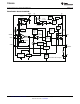
TPS54060A www.ti.com SLVSB57B – MARCH 2012 – REVISED SEPTEMBER 2013 DEVICE INFORMATION PIN CONFIGURATION MSOP-10 (TOP VIEW) VSON-10 (TOP VIEW) BOOT 1 10 PH VIN 2 EN 3 SS/TR 4 9 GND Thermal Pad (11) RT/CLK 5 8 COMP BOOT 1 VIN 2 10 Thermal Pad (11) PH 9 GND 8 COMP EN 3 7 VSENSE SS/TR 4 7 VSENSE 6 PWRGD RT/CLK 5 6 PWRGD PIN FUNCTIONS PIN I/O DESCRIPTION NAME NO. BOOT 1 O A bootstrap capacitor is required between BOOT and PH.
TPS54060A SLVSB57B – MARCH 2012 – REVISED SEPTEMBER 2013 www.ti.
TPS54060A www.ti.com SLVSB57B – MARCH 2012 – REVISED SEPTEMBER 2013 TYPICAL CHARACTERISTICS VOLTAGE REFERENCE vs JUNCTION TEMPERATURE 0.816 500 VI = 12 V VI = 12 V 375 Vref - Voltage Reference - V RDSON - Static Drain-Source On-State Resistance - mW ON RESISTANCE vs JUNCTION TEMPERATURE BOOT-PH = 3 V 250 BOOT-PH = 6 V 125 0 -50 0.808 0.800 0.792 0.784 -50 -25 0 25 50 75 100 TJ - Junction Temperature - °C 125 -25 0 150 Figure 1.
TPS54060A SLVSB57B – MARCH 2012 – REVISED SEPTEMBER 2013 www.ti.com TYPICAL CHARACTERISTICS (continued) EA TRANSCONDUCTANCE DURING SLOW START vs JUNCTION TEMPERATURE EA TRANSCONDUCTANCE vs JUNCTION TEMPERATURE 150 40 VI = 12 V VI = 12 V 130 110 gm - mA/V gm - mA/V 30 90 20 70 10 -50 -25 0 25 50 75 100 TJ - Junction Temperature - °C 125 50 -50 150 -25 0 25 50 75 100 125 150 TJ - Junction Temperature - °C Figure 7. Figure 8.
TPS54060A www.ti.com SLVSB57B – MARCH 2012 – REVISED SEPTEMBER 2013 TYPICAL CHARACTERISTICS (continued) SS/TR DISCHARGE CURRENT vs JUNCTION TEMPERATURE SWITCHING FREQUENCY vs VSENSE 120 100 VI = 12 V VI = 12 V, TJ = 25°C 80 % of Nominal fsw II(SS/TR) - mA 115 110 60 40 105 20 100 -50 0 -25 0 25 50 75 100 TJ - Junction Temperature - °C 125 150 0 SHUTDOWN SUPPLY CURRENT vs INPUT VOLTAGE (Vin) 2 TJ = 25°C I(VIN) - mA 1.5 1 0.5 1 0.
TPS54060A SLVSB57B – MARCH 2012 – REVISED SEPTEMBER 2013 www.ti.com TYPICAL CHARACTERISTICS (continued) PWRGD ON RESISTANCE vs JUNCTION TEMPERATURE PWRGD THRESHOLD vs JUNCTION TEMPERATURE 115 100 VI = 12 V PWRGD Threshold - % of Vref VI = 12 V RDSON - W 80 60 40 20 0 -50 VSENSE Rising 110 VSENSE Falling 105 100 VSENSE Rising 95 VSENSE Falling 90 -25 0 50 25 75 100 125 85 -50 150 -25 0 125 150 Figure 20.
TPS54060A www.ti.com SLVSB57B – MARCH 2012 – REVISED SEPTEMBER 2013 OVERVIEW The TPS54060A device is a 60-V, 0.5-A, step-down (buck) regulator with an integrated high side n-channel MOSFET. To improve performance during line and load transients the device implements a constant frequency, current mode control which reduces output capacitance and simplifies external frequency compensation design.
TPS54060A SLVSB57B – MARCH 2012 – REVISED SEPTEMBER 2013 www.ti.com DETAILED DESCRIPTION Fixed Frequency PWM Control The TPS54060A uses an adjustable fixed frequency, peak current mode control. The output voltage is compared through external resistors on the VSENSE pin to an internal voltage reference by an error amplifier which drives the COMP pin. An internal oscillator initiates the turn on of the high side power switch. The error amplifier output is compared to the high side power switch current.
TPS54060A www.ti.com SLVSB57B – MARCH 2012 – REVISED SEPTEMBER 2013 DETAILED DESCRIPTION (continued) VOUT(ac) IL PH Figure 25. Pulse Skip Mode Operation Low Dropout Operation and Bootstrap Voltage (BOOT) The TPS54060A has an integrated boot regulator, and requires a small ceramic capacitor between the BOOT and PH pins to provide the gate drive voltage for the high side MOSFET. The BOOT capacitor is refreshed when the high side MOSFET is off and the low side diode conducts.
TPS54060A SLVSB57B – MARCH 2012 – REVISED SEPTEMBER 2013 www.ti.com DETAILED DESCRIPTION (continued) voltage is greater than 2.1V, at which point the BOOT UVLO threshold is exceeded, and the device starts switching again until the desired output voltage is reached. This operating condition persists until the input voltage and/or the load current increases.
TPS54060A www.ti.com SLVSB57B – MARCH 2012 – REVISED SEPTEMBER 2013 DETAILED DESCRIPTION (continued) Adjusting the Output Voltage The output voltage is set with a resistor divider from the output node to the VSENSE pin. It is recommended to use 1% tolerance or better divider resistors. Start with a 10 kΩ for the R2 resistor and use the Equation 1 to calculate R1. To improve efficiency at light loads consider using larger value resistors.
TPS54060A SLVSB57B – MARCH 2012 – REVISED SEPTEMBER 2013 www.ti.com DETAILED DESCRIPTION (continued) TPS54060A VIN R1 Ihys I1 0.9 mA 2.9 mA + R2 EN 1.25 V R3 - VOUT Figure 29. Adding Additional Hysteresis R1 = R2 = VSTART - VSTOP V IHYS + OUT R3 (4) VENA VSTART - VENA V + I1 - ENA R1 R3 (5) Do not place a low-impedance voltage source with greater than 5 V directly on the EN pin.
TPS54060A www.ti.com SLVSB57B – MARCH 2012 – REVISED SEPTEMBER 2013 DETAILED DESCRIPTION (continued) Slow Start/Tracking Pin (SS/TR) The TPS54060A effectively uses the lower voltage of the internal voltage reference or the SS/TR pin voltage as the power-supply's reference voltage and regulates the output accordingly. A capacitor on the SS/TR pin to ground implements a slow start time. The TPS54060A has an internal pull-up current source of 2μA that charges the external slow start capacitor.
TPS54060A SLVSB57B – MARCH 2012 – REVISED SEPTEMBER 2013 www.ti.com DETAILED DESCRIPTION (continued) Sequencing Many of the common power supply sequencing methods can be implemented using the SS/TR, EN and PWRGD pins. The sequential method can be implemented using an open drain output of a power on reset pin of another device. The sequential method is illustrated in Figure 32 using two TPS54060A devices.
TPS54060A www.ti.com SLVSB57B – MARCH 2012 – REVISED SEPTEMBER 2013 DETAILED DESCRIPTION (continued) Figure 34 shows a method for ratio-metric start up sequence by connecting the SS/TR pins together. The regulator outputs will ramp up and reach regulation at the same time. When calculating the slow start time the pull up current source must be doubled in Equation 6. Figure 35 shows the results of Figure 34. TPS54060A EN VOUT 1 SS/TR PWRGD TPS54060A VOUT 2 EN R1 SS/ TR R2 PWRGD R3 R4 Figure 36.
TPS54060A SLVSB57B – MARCH 2012 – REVISED SEPTEMBER 2013 www.ti.com DETAILED DESCRIPTION (continued) Vout2 + deltaV Vssoffset R1 = ´ VREF Iss VREF ´ R1 R2 = Vout2 + deltaV - VREF deltaV = Vout1 - Vout2 R1 > 2800 ´ Vout1 - 180 ´ deltaV (7) (8) (9) (10) EN EN VOUT1 VOUT1 VOUT2 Figure 37. Ratio-metric Startup with Tracking Resistors VOUT2 Figure 38. Ratiometric Startup with Tracking Resistors EN VOUT1 VOUT2 Figure 39.
TPS54060A www.ti.com SLVSB57B – MARCH 2012 – REVISED SEPTEMBER 2013 DETAILED DESCRIPTION (continued) Constant Switching Frequency and Timing Resistor (RT/CLK Pin) The switching frequency of the TPS54060A is adjustable over a wide range from approximately 100kHz to 2500kHz by placing a resistor on the RT/CLK pin. The RT/CLK pin voltage is typically 0.5V and must have a resistor to ground to set the switching frequency.
TPS54060A SLVSB57B – MARCH 2012 – REVISED SEPTEMBER 2013 www.ti.com DETAILED DESCRIPTION (continued) Selecting the Switching Frequency The switching frequency that is selected should be the lower value of the two equations, Equation 12 and Equation 13. Equation 12 is the maximum switching frequency limitation set by the minimum controllable on time. Setting the switching frequency above this value will cause the regulator to skip switching pulses.
TPS54060A www.ti.com SLVSB57B – MARCH 2012 – REVISED SEPTEMBER 2013 DETAILED DESCRIPTION (continued) How to Interface to RT/CLK Pin The RT/CLK pin can be used to synchronize the regulator to an external system clock. To implement the synchronization feature connect a square wave to the RT/CLK pin through the circuit network shown in Figure 43. The square wave amplitude must transition lower than 0.5V and higher than 2.
TPS54060A SLVSB57B – MARCH 2012 – REVISED SEPTEMBER 2013 www.ti.com DETAILED DESCRIPTION (continued) PH PH EXT EXT IL IL Figure 44. Plot of Synchronizing in ccm Figure 45. Plot of Synchronizing in dcm PH EXT IL Figure 46. Plot of Synchronizing in PSM Power Good (PWRGD Pin) The PWRGD pin is an open drain output. Once the VSENSE pin is between 94% and 107% of the internal voltage reference the PWRGD pin is de-asserted and the pin floats.
TPS54060A www.ti.com SLVSB57B – MARCH 2012 – REVISED SEPTEMBER 2013 DETAILED DESCRIPTION (continued) Overvoltage Transient Protection The TPS54060A incorporates an overvoltage transient protection (OVTP) circuit to minimize voltage overshoot when recovering from output fault conditions or strong unload transients on power supply designs with low value output capacitance.
TPS54060A SLVSB57B – MARCH 2012 – REVISED SEPTEMBER 2013 www.ti.com DETAILED DESCRIPTION (continued) Simple Small Signal Model for Peak Current Mode Control Figure 48 describes a simple small signal model that can be used to understand how to design the frequency compensation. The TPS54060A power stage can be approximated to a voltage-controlled current source (duty cycle modulator) supplying current to the output capacitor and load resistor.
TPS54060A www.ti.com SLVSB57B – MARCH 2012 – REVISED SEPTEMBER 2013 DETAILED DESCRIPTION (continued) Equation 18 through Equation 27 are provided as a reference for those who prefer to compensate using the preferred methods. Those who prefer to use prescribed method use the method outlined in the application section or use switched information. VO R1 VSENSE gmea Type 2A COMP Type 2B Type 1 Vref R2 RO R3 CO C2 C1 R3 C2 C1 Figure 49.
TPS54060A SLVSB57B – MARCH 2012 – REVISED SEPTEMBER 2013 www.ti.
TPS54060A www.ti.com SLVSB57B – MARCH 2012 – REVISED SEPTEMBER 2013 APPLICATION INFORMATION Design Guide — Step-By-Step Design Procedure This example details the design of a high frequency switching regulator design using ceramic output capacitors. A few parameters must be known in order to start the design process. These parameters are typically determined at the system level. For this example, we will start with the following known parameters: Output Voltage 3.3 V Transient Response 0 to 0.
TPS54060A SLVSB57B – MARCH 2012 – REVISED SEPTEMBER 2013 www.ti.com Output Inductor Selection (LO) To calculate the minimum value of the output inductor, use Equation 28. KIND is a coefficient that represents the amount of inductor ripple current relative to the maximum output current. The inductor ripple current will be filtered by the output capacitor.
TPS54060A www.ti.com SLVSB57B – MARCH 2012 – REVISED SEPTEMBER 2013 to see the change in load current and output voltage and adjust the duty cycle to react to the change. The output capacitor must be sized to supply the extra current to the load until the control loop responds to the load change. The output capacitance must be large enough to supply the difference in current for 2 clock cycles while only allowing a tolerable amount of droop in the output voltage.
TPS54060A SLVSB57B – MARCH 2012 – REVISED SEPTEMBER 2013 www.ti.com V RESR < ORIPPLE IRIPPLE Icorms = (35) Vout ´ (Vin max - Vout) 12 ´ Vin max ´ Lo ´ ¦ sw (36) Catch Diode The TPS54060A requires an external catch diode between the PH pin and GND. The selected diode must have a reverse voltage rating equal to or greater than Vinmax. The peak current rating of the diode must be greater than the maximum inductor current. The diode should also have a low forward voltage.
TPS54060A www.ti.com Icirms = Iout ´ SLVSB57B – MARCH 2012 – REVISED SEPTEMBER 2013 Vout ´ Vin min (Vin min - Vout ) Vin min (38) Iout max ´ 0.25 ΔVin = Cin ´ ¦ sw (39) Table 1. Capacitor Types VENDOR VALUE (μF) 1.0 to 2.2 Murata 1.0 to 4.7 1.0 1.0 to 2.2 1.0 10 1.8 Vishay 1.0 to 1.2 1.0 to 3.9 1.0 to 1.8 1.0 to 2.2 TDK 1.5 to 6.8 1.0. to 2.2 1.0 to 3.3 1.0 to 4.7 AVX 1.0 1.0 to 4.7 1.0 to 2.
TPS54060A SLVSB57B – MARCH 2012 – REVISED SEPTEMBER 2013 www.ti.com Under Voltage Lock Out Set Point The Under Voltage Lock Out (UVLO) can be adjusted using an external voltage divider on the EN pin of the TPS54060A. The UVLO has two thresholds, one for power up when the input voltage is rising and one for power down or brown outs when the input voltage is falling. For the example design, the supply should turn on and start switching once the input voltage increases above 8.9V (enabled).
TPS54060A www.ti.com SLVSB57B – MARCH 2012 – REVISED SEPTEMBER 2013 æ 2 ´ p ´ fco ´ Cout R4 = ç gmps è ö ö æ Vout ÷ ÷´ç ´ V gmea ø è ref ø (45) 1 C7 = 2 ´ p ´ R4 ´ f p m od (46) Use the larger value of Equation 47 and Equation 48 to calculate the C8, to set the compensation pole. Equation 48 yields 8.7pF so the nearest standard of 10pF is used.
TPS54060A SLVSB57B – MARCH 2012 – REVISED SEPTEMBER 2013 www.ti.com Figure 56. Output Ripple, PSM Figure 57. Input Ripple CCM 100 90 80 Efficiency - % 70 VIN = 12 V 60 VIN = 24 V VIN = 18 V VIN = 34 V 50 VIN = 42 40 30 20 10 VOUT = 3.3 V 0 0 Figure 58. Input Ripple DCM 0.05 0.10 0.15 0.20 0.25 0.30 0.35 IO - Output Current - A 0.40 0.45 0.50 Figure 59.
TPS54060A www.ti.com SLVSB57B – MARCH 2012 – REVISED SEPTEMBER 2013 0.1 0.1 0.06 0.06 0.04 0.04 0.02 0 -0.02 0.02 0 -0.02 -0.04 -0.04 -0.06 -0.06 -0.08 -0.08 -0.1 0.00 IO = 0.25 A 0.08 VI = 34 V Regulation (%) Regulation (%) 0.08 -0.1 0.25 0.1 0.15 0.2 0.25 0.3 0.35 0.4 0.45 0.5 10 15 20 25 30 35 40 45 50 55 60 VI - Input Voltage - V Load Current - A Figure 62. Regulation vs Load Current Figure 63.
TPS54060A SLVSB57B – MARCH 2012 – REVISED SEPTEMBER 2013 www.ti.com Power Dissipation Estimate The following formulas show how to estimate the IC power dissipation under continuous conduction mode (CCM) operation. These equations should not be used if the device is working in discontinuous conduction mode (DCM). The power dissipation of the IC includes conduction loss (Pcon), switching loss (Psw), gate drive loss (Pgd) and supply current (Pq).
TPS54060A www.ti.com SLVSB57B – MARCH 2012 – REVISED SEPTEMBER 2013 Layout Layout is a critical portion of good power supply design. There are several signals paths that conduct fast changing currents or voltages that can interact with stray inductance or parasitic capacitance to generate noise or degrade the power supplies performance. To help eliminate these problems, the VIN pin should be bypassed to ground with a low ESR ceramic bypass capacitor with X5R or X7R dielectric.
TPS54060A SLVSB57B – MARCH 2012 – REVISED SEPTEMBER 2013 www.ti.com VIN + Cin Cboot Lo BOOT VIN Cd PH GND R1 + GND Co R2 TPS54060A VOUT VSENSE EN COMP SS/TR Rcomp RT/CLK Css Czero RT Cpole Figure 65. Inverting Power Supply from the SLVA317 Application Note VOPOS + VIN Copos + Cin Cboot BOOT VIN GND PH Lo Cd R1 GND + Coneg R2 TPS54060A VONEG VSENSE EN COMP SS/TR Rcomp RT/CLK Css RT Czero Cpole Figure 66.
TPS54060A www.ti.com SLVSB57B – MARCH 2012 – REVISED SEPTEMBER 2013 REVISION HISTORY Changes from Original (March 2012) to Revision A Page • Changed in DESCRIPTION second paragraph 93% to 94% ............................................................................................... 1 • Changed in the ABS MAX TABLE, row Elec Discharge (HBM), max value from 1 to 2 ...................................................... 2 • Deleted the second row in the Thermal Information table ..................
PACKAGE OPTION ADDENDUM www.ti.
PACKAGE OPTION ADDENDUM www.ti.com 15-Jun-2014 Important Information and Disclaimer:The information provided on this page represents TI's knowledge and belief as of the date that it is provided. TI bases its knowledge and belief on information provided by third parties, and makes no representation or warranty as to the accuracy of such information. Efforts are underway to better integrate information from third parties.
PACKAGE MATERIALS INFORMATION www.ti.com 16-Jun-2014 TAPE AND REEL INFORMATION *All dimensions are nominal Device Package Package Pins Type Drawing SPQ Reel Reel A0 Diameter Width (mm) (mm) W1 (mm) B0 (mm) K0 (mm) P1 (mm) W Pin1 (mm) Quadrant TPS54060ADGQR MSOPPower PAD DGQ 10 2500 330.0 12.4 5.3 3.3 1.3 8.0 12.0 Q1 TPS54060ADRCR SON DRC 10 3000 330.0 12.4 3.3 3.3 1.0 8.0 12.0 Q2 TPS54060ADRCT SON DRC 10 250 180.0 12.4 3.3 3.3 1.0 8.0 12.
PACKAGE MATERIALS INFORMATION www.ti.com 16-Jun-2014 *All dimensions are nominal Device Package Type Package Drawing Pins SPQ Length (mm) Width (mm) Height (mm) TPS54060ADGQR MSOP-PowerPAD DGQ 10 2500 346.0 346.0 35.0 TPS54060ADRCR SON DRC 10 3000 346.0 346.0 35.0 TPS54060ADRCT SON DRC 10 250 203.0 203.0 35.
IMPORTANT NOTICE Texas Instruments Incorporated and its subsidiaries (TI) reserve the right to make corrections, enhancements, improvements and other changes to its semiconductor products and services per JESD46, latest issue, and to discontinue any product or service per JESD48, latest issue. Buyers should obtain the latest relevant information before placing orders and should verify that such information is current and complete.