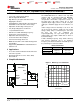
Product Folder Sample & Buy Support & Community Tools & Software Technical Documents TPS54160, TPS54160A SLVSB56C – MAY 2012 – REVISED FEBRUARY 2014 TPS54160 1.5-A, 60-V, Step-Down DC/DC Converter with Eco-mode™ 1 Features 3 Description • • • The TPS54160A device is a 60-V, 1.5-A, step down regulator with an integrated high-side MOSFET. Current mode control provides simple external compensation and flexible component selection.
TPS54160, TPS54160A SLVSB56C – MAY 2012 – REVISED FEBRUARY 2014 www.ti.com Table of Contents 1 2 3 4 5 6 7 8 Features .................................................................. Applications ........................................................... Description ............................................................. Simplified Schematic............................................. Revision History..................................................... Terminal Configuration and Functions....
TPS54160, TPS54160A www.ti.com SLVSB56C – MAY 2012 – REVISED FEBRUARY 2014 Changes from Original (May 2012) to Revision A Page • Changed text in the Description From: "within 93% to 107% of its nominal voltage." To: "within 94% to 107% of its nominal voltage." ....................................................................................................................................................................
TPS54160, TPS54160A SLVSB56C – MAY 2012 – REVISED FEBRUARY 2014 www.ti.com 6 Terminal Configuration and Functions MSOP-10 (TOP VIEW) VSON-10 (TOP VIEW) BOOT 1 10 PH VIN 2 9 GND Thermal Pad (11) EN 3 SS/TR 4 RT/CLK 5 8 COMP BOOT 1 VIN 2 10 Thermal Pad (11) PH 9 GND 8 COMP EN 3 7 VSENSE SS/TR 4 7 VSENSE 6 PWRGD RT/CLK 5 6 PWRGD Terminal Functions TERMINAL I/O DESCRIPTION NAME NO. BOOT 1 O A bootstrap capacitor is required between BOOT and PH.
TPS54160, TPS54160A www.ti.com SLVSB56C – MAY 2012 – REVISED FEBRUARY 2014 7 Specifications 7.1 Absolute Maximum Ratings (1) Over operating temperature range (unless otherwise noted). VALUE MIN MAX VIN –0.3 65 EN (2) –0.3 5 BOOT Input voltage 73 VSENSE –0.3 3 COMP –0.3 3 PWRGD –0.3 6 SS/TR –0.3 3 RT/CLK –0.3 3.6 –0.
TPS54160, TPS54160A SLVSB56C – MAY 2012 – REVISED FEBRUARY 2014 www.ti.com 7.3 Recommended Operating Conditions over operating free-air temperature range (unless otherwise noted) MIN MAX UNIT VIN Supply input voltage range 3.5 60 V VO Output voltage range 0.8 58 V IO Output current range 0 1.5 A TJ Junction Temperature –40 150 °C 7.4 Thermal Information TPS54160 TPS54160A THERMAL METRIC (1) UNITS DGQ (10 PINS) DRC (10 PINS) 62.
TPS54160, TPS54160A www.ti.com SLVSB56C – MAY 2012 – REVISED FEBRUARY 2014 Electrical Characteristics (continued) TJ = –40°C to 150°C, VIN = 3.5 to 60V (unless otherwise noted) PARAMETER TEST CONDITIONS MIN TYP MAX UNIT 1.8 2.
TPS54160, TPS54160A SLVSB56C – MAY 2012 – REVISED FEBRUARY 2014 www.ti.com 0.816 500 VI = 12 V VI = 12 V 375 BOOT-PH = 3 V 250 BOOT-PH = 6 V 125 0 -50 0.808 Vref - Voltage Reference - V RDSON - Static Drain-Source On-State Resistance - mW 7.6 Typical Characteristics 0.800 0.792 0.784 -50 -25 0 25 50 75 100 TJ - Junction Temperature - °C 125 -25 0 150 25 50 75 100 TJ - Junction Temperature - °C 125 150 Figure 3. Voltage Reference vs Junction Temperature Figure 2.
TPS54160, TPS54160A www.ti.com SLVSB56C – MAY 2012 – REVISED FEBRUARY 2014 Typical Characteristics (continued) 150 40 VI = 12 V VI = 12 V 130 110 gm - mA/V gm - mA/V 30 90 20 70 10 -50 -25 0 25 50 75 100 TJ - Junction Temperature - °C 125 50 -50 150 -25 0 25 50 75 100 125 150 TJ - Junction Temperature - °C Figure 8. EA Transconductance During SLOW Start vs Junction Temperature Figure 9. EA Transconductance vs Junction Temperature 1.40 -3.
TPS54160, TPS54160A SLVSB56C – MAY 2012 – REVISED FEBRUARY 2014 www.ti.com Typical Characteristics (continued) 120 100 VI = 12 V VI = 12 V, TJ = 25°C 80 % of Nominal fsw II(SS/TR) - mA 115 110 60 40 105 20 100 -50 0 -25 0 25 50 75 100 TJ - Junction Temperature - °C 125 150 0 Figure 14. SS/TR Discharge Current vs Junction Temperature 0.8 TJ = 25°C 1.5 1.5 I(VIN) - mA I(VIN) - mA 0.6 2 VI = 12 V 1 0.5 1 0.
TPS54160, TPS54160A www.ti.com SLVSB56C – MAY 2012 – REVISED FEBRUARY 2014 Typical Characteristics (continued) 115 100 VI = 12 V PWRGD Threshold - % of Vref VI = 12 V RDSON - W 80 60 40 20 VSENSE Rising 110 VSENSE Falling 105 100 VSENSE Rising 95 VSENSE Falling 90 0 -50 -25 0 25 50 75 100 125 85 -50 150 -25 0 TJ - Junction Temperature - °C 3 2.3 2.75 VI(VIN) - V VI(BOOT-PH) - V 2.5 1.8 150 2.50 2.25 1.
TPS54160, TPS54160A SLVSB56C – MAY 2012 – REVISED FEBRUARY 2014 www.ti.com 8 Detailed Description 8.1 Overview The TPS54160A device is a 60-V, 1.5-A, step-down (buck) regulator with an integrated high-side n-channel MOSFET. To improve performance during line and load transients the device implements a constant frequency, current mode control which reduces output capacitance and simplifies external frequency compensation design.
TPS54160, TPS54160A www.ti.com SLVSB56C – MAY 2012 – REVISED FEBRUARY 2014 8.
TPS54160, TPS54160A SLVSB56C – MAY 2012 – REVISED FEBRUARY 2014 www.ti.com Feature Description (continued) quiescent current. While the device is in sleep mode the output power is delivered by the output capacitor. As the load current decreases, the time the output capacitor supplies the load current increases and the switching frequency decreases reducing gate drive and switching losses.
TPS54160, TPS54160A www.ti.com SLVSB56C – MAY 2012 – REVISED FEBRUARY 2014 Feature Description (continued) The start and stop voltages are shown in Figure 27 and Figure 28. The voltages are plotted versus load current. The start voltage is defined as the input voltage needed to regulate the output within 1%. The stop voltage is defined as the input voltage at which the output drops by 5% or stops switching. 4 5.6 VO = 3.3 V VO = 5 V 5.4 VI - Input Voltage - V VI - Input Voltage - V 3.8 3.
TPS54160, TPS54160A SLVSB56C – MAY 2012 – REVISED FEBRUARY 2014 www.ti.com Feature Description (continued) TPS54160A VIN Ihys I1 0.9 mA R1 2.9 mA + R2 EN - 1.25 V Figure 29. Adjustable Undervoltage Lockout (UVLO) V - VSTOP R1 = START IHYS (2) VENA R2 = VSTART - VENA + I1 R1 (3) Another technique to add input voltage hysteresis is shown in Figure 30. This method may be used, if the resistance values are high from the previous method and a wider voltage hysteresis is needed.
TPS54160, TPS54160A www.ti.com SLVSB56C – MAY 2012 – REVISED FEBRUARY 2014 Feature Description (continued) VIN R1 Node ENA 10kohm R2 5.8V Figure 31.
TPS54160, TPS54160A SLVSB56C – MAY 2012 – REVISED FEBRUARY 2014 www.ti.com Feature Description (continued) 8.3.10 Slow Start and Tracking Pin (SS/TR) The TPS54160A effectively uses the lower voltage of the internal voltage reference or the SS/TR pin voltage as the power-supply's reference voltage and regulates the output accordingly. A capacitor on the SS/TR pin to ground implements a slow start time.
TPS54160, TPS54160A www.ti.com SLVSB56C – MAY 2012 – REVISED FEBRUARY 2014 Feature Description (continued) 8.3.12 Sequencing Many of the common power supply sequencing methods can be implemented using the SS/TR, EN and PWRGD pins. The sequential method can be implemented using an open drain output of a power on reset pin of another device. The sequential method is illustrated in Figure 33 using two TPS54160A devices.
TPS54160, TPS54160A SLVSB56C – MAY 2012 – REVISED FEBRUARY 2014 www.ti.com Feature Description (continued) TPS54160A 3 EN EN1, EN2 4 SS/TR 6 PWRGD VOUT1 VOUT2 TPS54160A 3 EN 4 SS/TR 6 PWRGD Figure 35. Schematic for Ratiometric Start-Up Using Coupled SS/TR Pins Figure 36. Ratio-Metric Startup using Coupled SS/TR pins Figure 35 shows a method for ratio-metric start up sequence by connecting the SS/TR pins together. The regulator outputs ramp up to reach regulation at the same time.
TPS54160, TPS54160A www.ti.com SLVSB56C – MAY 2012 – REVISED FEBRUARY 2014 Feature Description (continued) TPS54160A EN VOUT 1 SS/TR PWRGD TPS54160A VOUT 2 EN R1 SS/ TR R2 PWRGD R3 R4 Figure 37. Schematic for Ratiometric and Simultaneous Start-Up Sequence Ratio-metric and simultaneous power supply sequencing can be implemented by connecting the resistor network of R1 and R2 shown in Figure 37 to the output of the power supply that needs to be tracked or another voltage reference source.
TPS54160, TPS54160A SLVSB56C – MAY 2012 – REVISED FEBRUARY 2014 www.ti.com Feature Description (continued) R1 > 2800 ´ VOUT1 - 180 ´ DV (10) EN EN VOUT1 VOUT1 VOUT2 Figure 38. Ratiometric Startup with VOUT2 Leading VOUT1 VOUT2 Figure 39. Ratiometric Startup with VOUT1 Leading VOUT2 EN VOUT1 VOUT2 Figure 40.
TPS54160, TPS54160A www.ti.com SLVSB56C – MAY 2012 – REVISED FEBRUARY 2014 Feature Description (continued) 8.3.13 Constant Switching Frequency and Timing Resistor (RT/CLK Pin) The switching frequency of the TPS54160A is adjustable over a wide range from approximately 100kHz to 2500kHz by placing a resistor on the RT/CLK pin. The RT/CLK pin voltage is typically 0.5V and must have a resistor to ground to set the switching frequency.
TPS54160, TPS54160A SLVSB56C – MAY 2012 – REVISED FEBRUARY 2014 www.ti.com Feature Description (continued) 8.3.15 Selecting the Switching Frequency The switching frequency that is selected should be the lower value of the two equations, Equation 12 and Equation 13. Equation 12 is the maximum switching frequency limitation set by the minimum controllable on time. Setting the switching frequency above this value causes the regulator to skip switching pulses.
TPS54160, TPS54160A www.ti.com SLVSB56C – MAY 2012 – REVISED FEBRUARY 2014 Feature Description (continued) 8.3.16 How to Interface to RT/CLK Pin The RT/CLK pin can be used to synchronize the regulator to an external system clock. To implement the synchronization feature connect a square wave to the RT/CLK pin through the circuit network shown in Figure 44. The square wave amplitude must transition lower than 0.5V and higher than 2.
TPS54160, TPS54160A SLVSB56C – MAY 2012 – REVISED FEBRUARY 2014 www.ti.com Feature Description (continued) EXT EXT VOUT IL PH PH IL Figure 45. Plot of Synchronizing in CCM Figure 46. Plot of Synchronizing in DCM EXT IL PH Figure 47. Plot of Synchronizing in PSM 8.3.17 Power Good (PWRGD Pin) The PWRGD pin is an open drain output. Once the VSENSE pin is between 94% and 107% of the internal voltage reference the PWRGD pin is de-asserted and the pin floats.
TPS54160, TPS54160A www.ti.com SLVSB56C – MAY 2012 – REVISED FEBRUARY 2014 Feature Description (continued) 8.3.18 Overvoltage Transient Protection The TPS54160A incorporates an overvoltage transient protection (OVTP) circuit to minimize voltage overshoot when recovering from output fault conditions or strong unload transients on power supply designs with low value output capacitance.
TPS54160, TPS54160A SLVSB56C – MAY 2012 – REVISED FEBRUARY 2014 www.ti.com Feature Description (continued) 8.3.21 Simple Small Signal Model for Peak Current Mode Control Figure 49 describes a simple small signal model that can be used to understand how to design the frequency compensation. The TPS54160A power stage can be approximated to a voltage-controlled current source (duty cycle modulator) supplying current to the output capacitor and load resistor.
TPS54160, TPS54160A www.ti.com SLVSB56C – MAY 2012 – REVISED FEBRUARY 2014 Feature Description (continued) 8.3.22 Small Signal Model for Frequency Compensation The TPS54160A uses a transconductance amplifier for the error amplifier and readily supports three of the commonly-used frequency compensation circuits. Compensation circuits Type 2A, Type 2B, and Type 1 are shown in Figure 50. Type 2 circuits most likely implemented in high bandwidth power-supply designs using low ESR output capacitors.
TPS54160, TPS54160A SLVSB56C – MAY 2012 – REVISED FEBRUARY 2014 www.ti.
TPS54160, TPS54160A www.ti.com SLVSB56C – MAY 2012 – REVISED FEBRUARY 2014 9 Application and Implementation 9.1 Application Information TPS5426x devices are part of a family of non-synchronous, step-down converters with an integrated high-side FET and 100% duty cycle capability. Idea applications are 12-V, 24-V and 48-V industrial and commercial low power systems. Aftermarket Auto Accessories: Video, GPS, Entertainment 9.2 Typical Application L1 10 mH U1 TPS54160ADGQ BOOT VIN C2 C3 C4 2.2 mF 2.
TPS54160, TPS54160A SLVSB56C – MAY 2012 – REVISED FEBRUARY 2014 www.ti.com The typical minimum on time, tonmin, is 130 ns for the TPS54160A. For this example, the output voltage is 3.3 V and the maximum input voltage is 18 V, which allows for a maximum switch frequency up to 1600 kHz when including the inductor resistance, on resistance and diode voltage in Equation 12.
TPS54160, TPS54160A www.ti.com SLVSB56C – MAY 2012 – REVISED FEBRUARY 2014 9.2.2.3 Output Capacitor There are three primary considerations for selecting the value of the output capacitor. The output capacitor will determine the modulator pole, the output voltage ripple, and how the regulators responds to a large change in load current. The output capacitance needs to be selected based on the more stringent of these three criteria.
TPS54160, TPS54160A SLVSB56C – MAY 2012 – REVISED FEBRUARY 2014 www.ti.com 1 1 ´ 8 ´ fSW æ VOUT(ripple ) ö ç ÷ ç IRIPPLE ÷ è ø (34) COUT > VOUT(ripple ) RESR = IRIPPLE ICOUT(rms) = (35) ( VOUT ´ VIN(max ) - VOUT ) 12 ´ VIN(max ) ´ LO ´ fSW (36) 9.2.2.4 Catch Diode The TPS54160A requires an external catch diode between the PH pin and GND. The selected diode must have a reverse voltage rating equal to or greater than Vinmax.
TPS54160, TPS54160A www.ti.com SLVSB56C – MAY 2012 – REVISED FEBRUARY 2014 For this example design, a ceramic capacitor with at least a 20 V voltage rating is required to support the maximum input voltage. Common standard ceramic capacitor voltage ratings include 4 V, 6.3 V, 10 V, 16 V, 25 V, 50 V or 100 V, so a 25 V capacitor should be selected. For this example, two 2.2 μF, 25 V capacitors in parallel have been selected. Table 2 shows a selection of high voltage capacitors.
TPS54160, TPS54160A SLVSB56C – MAY 2012 – REVISED FEBRUARY 2014 www.ti.com Once the slow start time is known, the slow start capacitor value can be calculated using Equation 6. For the example circuit, the slow start time is not too critical since the output capacitor value is 47μF which does not require much current to charge to 3.3V. The example circuit has the slow start time set to an arbitrary value of 1ms which requires a 3.3 nF capacitor. ´ VOUT ´ 0.8 C tSS > OUT ISS(avg) (40) 9.2.2.
TPS54160, TPS54160A www.ti.com SLVSB56C – MAY 2012 – REVISED FEBRUARY 2014 where • • • IOUT(max) is the maximum output current COUT is the output capacitance VOUT is the nominal output voltage f Z(mod) = (41) 1 2 ´ p ´ RESR ´ COUT (42) For the example design, the modulator pole is located at 1.5 kHz and the ESR zero is located at 338 kHz. Next, the designer selects a crossover frequency which will determine the bandwidth of the control loop.
TPS54160, TPS54160A SLVSB56C – MAY 2012 – REVISED FEBRUARY 2014 CC = www.ti.
TPS54160, TPS54160A www.ti.com SLVSB56C – MAY 2012 – REVISED FEBRUARY 2014 TA (max ) = TJ(max ) - RTH ´ PTOT where • • • • • • PTOT s the total device power dissipation (W) TA is the ambient temperature (°C) TJ is the junction temperature (°C) RTH is the thermal resistance of the package (°C/W) TJ(max) is maximum junction temperature (°C) TA(max) is maximum ambient temperature (°C).
TPS54160, TPS54160A SLVSB56C – MAY 2012 – REVISED FEBRUARY 2014 www.ti.com 9.2.3 Application Curves VIN VO VOUT EN IO IL Figure 53. Load Transmit Figure 54. Startup With EN VOUT VOUT IL PH VIN IL Figure 55. VIN Power Up Figure 56. Output Ripple CCM VOUT VOUT IL IL PH Figure 57. Output Ripple, DCM 40 Submit Documentation Feedback PH Figure 58.
TPS54160, TPS54160A www.ti.com SLVSB56C – MAY 2012 – REVISED FEBRUARY 2014 VIN VIN IL IL PH PH Figure 60. Input Ripple DCM Figure 59. Input Ripple CCM 95 VO = 3.3 V, fsw = 1200 kHz VI = 8 V 90 85 VIN Efficiency - % 80 IL VI = 12 V 75 VI = 16 V 70 65 PH 60 55 50 0 0.25 0.50 0.75 1 1.25 IL - Load Current - A 1.5 1.75 2 Figure 62. Efficiency vs Load Current Figure 61. Input Ripple PSM 1.015 60 150 VI = 12 V 1.010 40 100 1.
TPS54160, TPS54160A SLVSB56C – MAY 2012 – REVISED FEBRUARY 2014 www.ti.com 1.015 IO = 0.5 A 1.010 Regulation (%) 1.005 1.000 0.995 0.990 0.985 5 10 15 20 VI - Input Voltage - V Figure 65. Regulation vs Input Voltage 10 Power Supply Recommendations The devices are designed to operate from an input voltage supply range between 3.5 V and 60 V. This input supply should be well regulated.
TPS54160, TPS54160A www.ti.com SLVSB56C – MAY 2012 – REVISED FEBRUARY 2014 11 Layout 11.1 Layout Guidelines Layout is a critical portion of good power supply design. There are several signals paths that conduct fast changing currents or voltages that can interact with stray inductance or parasitic capacitance to generate noise or degrade the power supplies performance.
TPS54160, TPS54160A SLVSB56C – MAY 2012 – REVISED FEBRUARY 2014 www.ti.com 12 Device and Documentation Support 12.1 Related Links The table below lists quick access links. Categories include technical documents, support and community resources, tools and software, and quick access to sample or buy. Table 3.
PACKAGE OPTION ADDENDUM www.ti.
PACKAGE OPTION ADDENDUM www.ti.com (4) 17-May-2014 There may be additional marking, which relates to the logo, the lot trace code information, or the environmental category on the device. (5) Multiple Device Markings will be inside parentheses. Only one Device Marking contained in parentheses and separated by a "~" will appear on a device. If a line is indented then it is a continuation of the previous line and the two combined represent the entire Device Marking for that device.
PACKAGE MATERIALS INFORMATION www.ti.com 31-May-2014 TAPE AND REEL INFORMATION *All dimensions are nominal Device Package Package Pins Type Drawing SPQ Reel Reel A0 Diameter Width (mm) (mm) W1 (mm) B0 (mm) K0 (mm) P1 (mm) W Pin1 (mm) Quadrant TPS54160ADGQR MSOPPower PAD DGQ 10 2500 330.0 12.4 5.3 3.4 1.4 8.0 12.0 Q1 TPS54160ADGQR MSOPPower PAD DGQ 10 2500 330.0 12.4 5.3 3.3 1.3 8.0 12.0 Q1 TPS54160ADRCR SON DRC 10 3000 330.0 12.4 3.3 3.3 1.0 8.0 12.
PACKAGE MATERIALS INFORMATION www.ti.com 31-May-2014 *All dimensions are nominal Device Package Type Package Drawing Pins SPQ Length (mm) Width (mm) Height (mm) TPS54160ADGQR MSOP-PowerPAD DGQ 10 2500 364.0 364.0 27.0 TPS54160ADGQR MSOP-PowerPAD DGQ 10 2500 346.0 346.0 35.0 TPS54160ADRCR SON DRC 10 3000 346.0 346.0 35.0 TPS54160ADRCT SON DRC 10 250 203.0 203.0 35.0 TPS54160DGQR MSOP-PowerPAD DGQ 10 2500 364.0 364.0 27.
IMPORTANT NOTICE Texas Instruments Incorporated and its subsidiaries (TI) reserve the right to make corrections, enhancements, improvements and other changes to its semiconductor products and services per JESD46, latest issue, and to discontinue any product or service per JESD48, latest issue. Buyers should obtain the latest relevant information before placing orders and should verify that such information is current and complete.