
Datasheet


1 Introduction
1.1 Background
1.2 Performance Specification Summary
Introduction
www.ti.com
This user's guide contains background information for the TPS54233 as well as support documentation for
the TPS54233EVM-373 evaluation module (HPA373). Also included are the performance specifications,
the schematic, and the bill of materials for the TPS54233EVM-373.
The TPS54233 dc/dc converter is designed to provide up to a 2 A output from an input voltage source of
3.5 V to 28 V. Rated input voltage and output current range for the evaluation module are given in
Table 1 . This evaluation module is designed to demonstrate the small printed-circuit-board areas that may
be achieved when designing with the TPS54233 regulator. The switching frequency is internally set at a
nominal 300 kHz. The high-side MOSFET is incorporated inside the TPS54233 package along with the
gate drive circuitry. The low drain-to-source on resistance of the MOSFET allows the TPS54233 to
achieve high efficiencies and helps keep the junction temperature low at high output currents. The
compensation components are external to the integrated circuit (IC), and an external divider allows for an
adjustable output voltage. Additionally, the TPS54233 provides adjustable slow start and undervoltage
lockout inputs. The absolute maximum input voltage is 30 V for the TPS54233EVM-373.
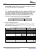
Table 1. Input Voltage and Output Current Summary
EVM INPUT VOLTAGE RANGE OUTPUT CURRENT RANGE
TPS54233EVM-373 VIN = 8 V to 18 V 0 A to 2 A
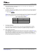
A summary of the TPS54233EVM-373 performance specifications is provided in Table 2 . Specifications
are given for an input voltage of V
IN
= 15 V and an output voltage of 3.3 V, unless otherwise specified.
The TPS54233EVM-373 is designed and tested for V
IN
= 7 V to 28 V. The ambient temperature is 25 ° C
for all measurements, unless otherwise noted.
Table 2. TPS54233EVM-373 and Performance Specification Summary
SPECIFICATION TEST CONDITIONS MIN TYP MAX UNIT
V
IN
voltage range 7 15 18 V
Output voltage set point 3.3 V
Output current range V
IN
= 8 V to 18 V 0 2 A
Line regulation I
O
= 1 A, V
IN
= 8V to 18 V ± 0.025%
Load regulation V
IN
= 15 V, I
O
= 0 A to 2 A ± 0.03%
Load transient response I
O
= 0.5 A to 1.5 A Voltage change –20 mV
Recovery time 400 µ s
I
O
= 1.5 A to 0.5 A Voltage change 20 mV
Recovery time 400 µ s
Loop bandwidth V
IN
= 15 V, I
O
= 1 A 9.0 kHz
Phase margin V
IN
= 15 V , I
O
= 1 A 70 °
Input ripple voltage I
O
= 2 A 250 mVpp
Output ripple voltage I
O
= 2 A 70 mVpp
Output rise time 3.5 ms
Operating frequency 300 kHz
Maximum efficiency TPS54233EVM-373, V
IN
= 8 V, I
O
= 0.4 A 91.2%
2 TPS54233EVM-373 2-A, SWIFT™ Regulator Evaluation Module SLVU264 – November 2008
Submit Documentation Feedback