TPS54262-Q1 www.ti.com SLVS996C – SEPTEMBER 2009 – REVISED JUNE 2010 2-A 60-V STEP-DOWN DC/DC CONVERTER WITH LOW QUIESCENT CURRENT Check for Samples: TPS54262-Q1 FEATURES 1 • • • • • • • • • • • • • Asynchronous Switch Mode Regulator 3.6 V to 48 V Operating Range, Withstands Transients up to 60 V 2 A Maximum Load Current 50 µA Typical Quiescent Current 200 kHz to 2.2 MHz Switching Frequency 0.8 V ± 1.
TPS54262-Q1 SLVS996C – SEPTEMBER 2009 – REVISED JUNE 2010 www.ti.com This integrated circuit can be damaged by ESD. Texas Instruments recommends that all integrated circuits be handled with appropriate precautions. Failure to observe proper handling and installation procedures can cause damage. ESD damage can range from subtle performance degradation to complete device failure.
TPS54262-Q1 www.ti.com SLVS996C – SEPTEMBER 2009 – REVISED JUNE 2010 RECOMMENDED OPERATING CONDITIONS VI MIN MAX 3.6 48 V In continuous conduction mode (CCM) 0.9 18 V Power up in low-power mode (LPM) or discontinuous conduction mode (DCM) 0.9 5.5 V Bootstrap capacitor (BOOT) 3.6 56 V Switched outputs (PH) Unregulated buck supply input voltage (VIN, EN) VReg Regulated output voltage 3.6 48 V Logic levels (RST, VSENSE, OV_TH, RST_TH, Rslew, SYNC, RT) 0 5.
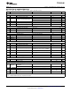
TPS54262-Q1 SLVS996C – SEPTEMBER 2009 – REVISED JUNE 2010 www.ti.com DC ELECTRICAL CHARACTERISTICS VIN = 7 V to 48 V, EN = VIN, TJ = –40°C to 150°C (unless otherwise noted) TEST PARAMETER TEST CONDITIONS MIN TYP MAX UNIT INPUT POWER SUPPLY Normal mode: after initial start up Info VIN Supply voltage on VIN Low-power mode 3.6 Iq-Normal Quiescent current, normal mode Iq-LPM Quiescent current, low-power mode V Rising threshold (LPM activated) 8.
TPS54262-Q1 www.ti.com SLVS996C – SEPTEMBER 2009 – REVISED JUNE 2010 DC ELECTRICAL CHARACTERISTICS VIN = 7 V to 48 V, EN = VIN, TJ = –40°C to 150°C (unless otherwise noted) TEST PARAMETER TEST CONDITIONS MIN TYP MAX UNIT ENABLE (EN) PT VIL Low input threshold voltage PT VIH High input threshold voltage PT Ilkg Leakage current into EN terminal 0.7 1.7 V V EN = 60 V 100 135 µA EN = 12 V 8 15 µA 2 2.
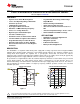
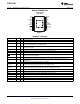
TPS54262-Q1 SLVS996C – SEPTEMBER 2009 – REVISED JUNE 2010 www.ti.com DEVICE INFORMATION PWP PACKAGE (TOP VIEW) NC NC SYNC LPM EN RT Rslew RST Cdly GND 1 20 2 19 3 18 4 17 5 16 6 15 7 14 8 13 9 12 10 11 BOOT VIN VIN PH VReg COMP VSENSE RST_TH OV_TH SS Figure 3. TERMINAL FUNCTIONS NAME NO. I/O NC 1 NC Connect to ground. NC 2 NC Connect to ground. SYNC 3 I External synchronization clock input to override the internal oscillator clock.
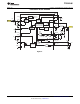
TPS54262-Q1 www.ti.com SLVS996C – SEPTEMBER 2009 – REVISED JUNE 2010 FUNCTIONAL BLOCK DIAGRAM BOOT 20 Bandgap ref LPM 4 D1 VIN 18 VBATT 0.8 V ref 0.2 V ref 7 R7 Internal supply Internal Voltage Rail 19 16 R11 C1 Gate Drive with Over-Current Limit for Internal Switch 5 R10 EN RT R8 6 Rslew Selectable Oscillator VIN VReg L PH 17 Thermal Sensor D2 ref Error amp SYNC 3 Cdly C2 14 + 0.8 V ref 11 RST GND + 0.8 V ref - 8 Reset with Delay Timer C4 C7 Voltage comp SS 15 0.
TPS54262-Q1 SLVS996C – SEPTEMBER 2009 – REVISED JUNE 2010 www.ti.com TYPICAL CHARACTERISTICS Efficiency Data of Power Supply 8 FET SWITCHING FAST SLEW RATE ON SWITCHING FET Figure 5. Figure 6. LPM, QUIESCENT CURRENT VARIATION WITH TEMPERATURE SHUTDOWN CURRENT VARIATION WITH TEMPERATURE Figure 7. Figure 8.
TPS54262-Q1 www.ti.com SLVS996C – SEPTEMBER 2009 – REVISED JUNE 2010 TYPICAL CHARACTERISTICS (continued) Output Voltage Drop Out VReg DROP OUT OUTPUT VOLTAGE TRACKING Figure 9. Figure 10. NOTE • • • Power up (Start up): This curve shows the input voltage required to achieve the 5 V regulation during power up over the range of load currents (see Figure 10). Power down (Tracking): This curve shows the input voltage at which the output voltage drops approximately by 0.
TPS54262-Q1 SLVS996C – SEPTEMBER 2009 – REVISED JUNE 2010 www.ti.com TYPICAL CHARACTERISTICS (continued) INTERNAL REFERENCE VOLTAGE VOLTAGE DROP ON Rslew FOR CURRENT REFERENCE; (SLEW RATE / Rslew) Figure 11. Figure 12. CURRENT CONSUMPTION WITH TEMPERATURE Figure 13.
TPS54262-Q1 www.ti.com SLVS996C – SEPTEMBER 2009 – REVISED JUNE 2010 OVERVIEW The TPS54262 is a 60 V, 2 A DC/DC step down (buck) converter using voltage-control mode scheme. The device features supervisory function for power-on-reset during system power on. Once the output voltage has exceeded the threshold set by RST_TH pin, a delay of 1 ms/nF (based on capacitor value on Cdly terminal) is invoked before the RST line is released high.
TPS54262-Q1 SLVS996C – SEPTEMBER 2009 – REVISED JUNE 2010 • • www.ti.com When VIN is less than typical VIN falling threshold level while LPM is disabled. From device specifications, VIN typical falling threshold (LPM disabled) = 8 V (see DC Electrical Characteristics). When RST is low. Regulation/Feedback Voltage The regulated output voltage (VReg) can be programmed by connecting external resistor network at VSENSE pin (pin 14). The output voltage is selectable between 0.
TPS54262-Q1 www.ti.com SLVS996C – SEPTEMBER 2009 – REVISED JUNE 2010 1) Active Mode Continuous Conduction Mode (CCM) In this mode of operation the switcher operates in continuous conduction mode, and the inductor current is always non-zero if the total load current (internal and external) is greater than IL_DISCONT shown in Equation 3. IL_DISCONT =IL_LPM = (1-D)×VReg 2×fsw ×L (3) Where, D = duty cycle L = output inductor VReg = output voltage fsw = switching frequency For VIN < 8.
TPS54262-Q1 SLVS996C – SEPTEMBER 2009 – REVISED JUNE 2010 www.ti.com Figure 17. Active Mode CCM • • Figure 18. PSM at Low VIN Likewise, at higher input voltages when the ON time (tON) of the switching FET becomes close to or slightly less than the minimum ON time (tON-Min) and the VReg start losing regulation, the device enters in PSM. If ON time is much smaller than tON-Min, there is a risk that the part stops switching and regulation is lost until power is re-cycled with ON time greater than tON-Min.
TPS54262-Q1 www.ti.com SLVS996C – SEPTEMBER 2009 – REVISED JUNE 2010 Figure 20. Low Power Mode Figure 21. Low Power Mode (Zoom In) Any transition from low-power mode to active mode CCM occurs within 5 µs (typical). In low-power mode, the converter operates as a hysteretic controller with the threshold limits set by VReg_UV (see Equation 10, Figure 4 and Figure 22), for the lower limit and ~VReg for the upper limit.
TPS54262-Q1 SLVS996C – SEPTEMBER 2009 – REVISED JUNE 2010 www.ti.com 5) Hysteretic Mode The device enters in this mode of operation when the main loop fails to respond during line/ load transients and regulate within specified tolerances. The device exits this mode of operation when the main control loop responds, after the error amplifier stabilizes, and controls the output voltage within tighter tolerance. The power up conditions in different modes of operations are explained in Table 4. Table 4.
TPS54262-Q1 www.ti.com SLVS996C – SEPTEMBER 2009 – REVISED JUNE 2010 Enable and Shutdown The EN pin (pin 5) provides electrical ON/OFF control of the regulator. Once the EN pin voltage exceeds the upper threshold voltage (VIH), the regulator starts operating and the internal soft start begins to ramp. If the EN pin voltage is pulled below the lower threshold voltage (VIL), the regulator stops switching and the internal soft start resets.
TPS54262-Q1 SLVS996C – SEPTEMBER 2009 – REVISED JUNE 2010 www.ti.com (7) Where, fsw-Max = maximum switching frequency tON-Min = minimum on-time of the NMOS switching transistor Knowing the switching frequency, the value of resistor to be connected at RT pin can be calculated using the graph shown in Figure 23. Figure 23.
TPS54262-Q1 www.ti.com SLVS996C – SEPTEMBER 2009 – REVISED JUNE 2010 Synchronization With External Clock An external clock signal can be supplied to the device through SYNC pin (pin 3) to synchronize the internal oscillator frequency with an external clock frequency. The synchronization input overrides the internal fixed oscillator signal. The synchronization signal has to be valid for approximately two clock cycles before the transition is made for synchronization with the external frequency input.
TPS54262-Q1 SLVS996C – SEPTEMBER 2009 – REVISED JUNE 2010 www.ti.com Power On Condition/ Reset Line Power Down Condition/ Reset Line VIN VIN Css Css VReg_RST VReg VReg Cdly Cdly VReg_RST tdelay RST RST 20 ms (Typ-Deglitch Time) Figure 26. Figure 27. Reset Delay The delay time to assert the RST pin high after the supply has exceeded the programmed VReg_RST voltage (see Equation 11 to calculate VReg_RST) can be set by external capacitor (C2 in Figure 4) connected to the Cdly pin (pin 9).
TPS54262-Q1 www.ti.com SLVS996C – SEPTEMBER 2009 – REVISED JUNE 2010 Overvoltage Supervisor The overvoltage monitoring of the regulated output voltage, VReg can be achieved by connecting an external resistor string to the OV_TH pin (pin 12). The resistor combination of R1, R2, and R3 is used to program the threshold for detection of overvoltage. The bias voltage of R3 sets the overvoltage threshold and the accuracy of regulated output voltage in hysteretic mode during transient events.
TPS54262-Q1 SLVS996C – SEPTEMBER 2009 – REVISED JUNE 2010 www.ti.com Loop Control Frequency Compensation Figure 28. Type 3 Compensation Type 3 Compensation Type 3 compensation has been used in the feedback loop to improve the stability of the convertor and regulation in the output in response to the changes in input voltage or load conditions. This becomes important because the ceramic capacitors used to filter the output have a low Equivalent Series Resistance (ESR).
TPS54262-Q1 www.ti.com SLVS996C – SEPTEMBER 2009 – REVISED JUNE 2010 For VIN = 8 V to 50 V, the VIN/Vramp modulator gain is approximately 10 and has a tolerance of about 20%. Gain = Amod = VIN = 10 Vramp (19) Therefore, (20) Also, Vramp is fixed for the following range of VIN. Vramp = 1 V for VIN < 8 V, and Vramp = 5 V for VIN > 48 V. The frequencies for poles and zeros are given by following equations.
TPS54262-Q1 SLVS996C – SEPTEMBER 2009 – REVISED JUNE 2010 www.ti.com Thermal Shutdown (TSD) The TPS54262 protects itself from overheating with an internal thermal shutdown (TSD) circuit. If the junction temperature exceeds the thermal shutdown trip point, the NMOS switching FET is turned off. The device is automatically restarted under the control of soft-start circuit when the junction temperature drops below the thermal shutdown hysteretic trip point.
TPS54262-Q1 www.ti.com SLVS996C – SEPTEMBER 2009 – REVISED JUNE 2010 For device under operation at a given ambient temperature (TA), the junction temperature (TJ) can be calculated using Equation 30. TJ = TA + (Rth × PTotal) (30) (30) Therefore, the rise in junction temperature due to power dissipation is shown in Equation 31.
TPS54262-Q1 SLVS996C – SEPTEMBER 2009 – REVISED JUNE 2010 www.ti.com APPLICATION INFORMATION These guidelines address the following topics in detail for TPS54262-Q1. 1. Component selection 2. Design example 3. PCB layout guidelines Component Selection This section explains considerations for the external components selection. The following schematic shows the interconnection between external components and the device for a typical DC/DC step down application.
TPS54262-Q1 www.ti.com SLVS996C – SEPTEMBER 2009 – REVISED JUNE 2010 2) Output Capacitor (C4, C12) The selection of the output capacitor will determine several parameters in the operation of the converter, for example voltage drop on the output capacitor and the output ripple. The capacitor value also determines the modulator pole and the roll-off frequency due to the LC output filter double pole. This is expressed in Equation 15.
TPS54262-Q1 SLVS996C – SEPTEMBER 2009 – REVISED JUNE 2010 www.ti.com 5) Power-On Reset Delay (PORdly) Capacitor (C2) The value of this capacitor can be calculated using Equation 9. 6) Output Inductor (L1) Use a low EMI inductor with a ferrite type shielded core. Other types of inductors may be used; however, they must have low EMI characteristics and should be located away from the low-power traces and components in the circuit.
TPS54262-Q1 www.ti.com SLVS996C – SEPTEMBER 2009 – REVISED JUNE 2010 9) Resistor to Select Switching Frequency (R8) Please refer to the section Selecting Switching Frequency, Figure 23 and Equation 7. 10) Resistors to Select Output Voltage (R4, R5) To minimize the effect of leakage current on the VSENSE terminal, the current flowing through the feedback network should be greater than 5 mA to maintain output accuracy.
TPS54262-Q1 SLVS996C – SEPTEMBER 2009 – REVISED JUNE 2010 www.ti.com (47) Capacitors Using Equation 23, C5 can be calculated as shown in Equation 48: (48) C7 can be calculated as shown in Equation 49: (49) C8 can be calculated as shown in Equation 50: (50) 14) Noise Filter on RST_TH and OV_TH Terminals (C9, C10) These capacitors may be required in some applications to filter the noise on RST_TH and OV_TH pins.
TPS54262-Q1 www.ti.com SLVS996C – SEPTEMBER 2009 – REVISED JUNE 2010 DESIGN EXAMPLE The following examples demonstrate the design of a high frequency switching regulator using ceramic output capacitors. A few parameters must be known to start the design process. These parameters are typically determined at the system level. Example 1 For this example, we will start with the following known and target parameters: Table 7.
TPS54262-Q1 SLVS996C – SEPTEMBER 2009 – REVISED JUNE 2010 www.ti.com Step 4. Calculate the Output Capacitor and ESR (C4) Calculate capacitance To calculate the capacitance of the output capacitor, minimum load current must be first determined. Typically, in standby mode the load current is 100 µA, however this really depends on the application. With this value of minimum load current and using Equation 35, Equation 36, and Equation 37, C4 is calculated to be, C4 > 34 µF .
TPS54262-Q1 www.ti.com SLVS996C – SEPTEMBER 2009 – REVISED JUNE 2010 Step 11. Calculate Resistors to Control Slew Rate (R7) The value of slew rate resistor (R7) can be approximately determined from Figure 24 and Figure 25 at different typical input voltages. The minimum recommended value is 10 kΩ. To achieve rise time, tr = 20 ns and fall time, tf = 35 ns, the slew rate resistor is approximately of value 30 kΩ. Step 12.
TPS54262-Q1 SLVS996C – SEPTEMBER 2009 – REVISED JUNE 2010 www.ti.com Example 2 For this example, we will start with the following known and target parameters: Table 8. Known Target Input voltage, VIN minimum=8 V, maximum= 28 V, typical=14 V Output voltage, VReg 3.
TPS54262-Q1 www.ti.com SLVS996C – SEPTEMBER 2009 – REVISED JUNE 2010 Calculate ESR Using Equation 38, ESR is calculated to be, RESR < 330 mΩ. Capacitors with lowest ESR values should be selected. To meet both the requirements, capacitance and low ESR, several low ESR capacitors may be connected in parallel. In this example, we will select a capacitor with ESR value as 30 mΩ. Filter capacitor (C12) of value 0.1µF can be added to filter out the noise in the output line. Step 5.
TPS54262-Q1 SLVS996C – SEPTEMBER 2009 – REVISED JUNE 2010 www.ti.com VReg_OV = 106% of VReg = 3.498 V VReg_RST = 92% of VReg = 3.036 V VReg_UV = 95% of VReg = 3.135 V Using Equation 12, R3 = 22.87 kΩ. Using Equation 11, R2 = 3.48 kΩ. Using Equation 10, R1 = 73.65 kΩ Step 13. Diode D1 and D2 Selection Diode D1 is used to protect the IC from the reverse input polarity connection. The diode should be rated at maximum load current. Only Schottky diode should be connected at the PH pin.
TPS54262-Q1 www.ti.com SLVS996C – SEPTEMBER 2009 – REVISED JUNE 2010 PCB LAYOUT GUIDELINES The following guidelines are recommended for PCB layout of the TPS54262 device. Traces and Ground Place Routing All power (high current) traces should be thick and as short as possible. The inductor and output capacitors should be as close to each other as possible. This will reduce EMI radiated by the power traces due to high switching currents.
PACKAGE OPTION ADDENDUM www.ti.com 17-Jun-2010 PACKAGING INFORMATION Orderable Device TPS54262QPWPRQ1 Status (1) ACTIVE Package Type Package Drawing HTSSOP PWP Pins Package Qty 20 2000 Eco Plan (2) Green (RoHS & no Sb/Br) Lead/ Ball Finish MSL Peak Temp (3) CU NIPDAU Level-3-260C-168 HR Samples (Requires Login) Request Free Samples (1) The marketing status values are defined as follows: ACTIVE: Product device recommended for new designs.
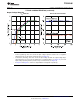
PACKAGE MATERIALS INFORMATION www.ti.com 14-Jul-2012 TAPE AND REEL INFORMATION *All dimensions are nominal Device TPS54262QPWPRQ1 Package Package Pins Type Drawing SPQ HTSSOP 2000 PWP 20 Reel Reel A0 Diameter Width (mm) (mm) W1 (mm) 330.0 16.4 Pack Materials-Page 1 6.95 B0 (mm) K0 (mm) P1 (mm) 7.1 1.6 8.0 W Pin1 (mm) Quadrant 16.
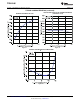
PACKAGE MATERIALS INFORMATION www.ti.com 14-Jul-2012 *All dimensions are nominal Device Package Type Package Drawing Pins SPQ Length (mm) Width (mm) Height (mm) TPS54262QPWPRQ1 HTSSOP PWP 20 2000 367.0 367.0 38.
IMPORTANT NOTICE Texas Instruments Incorporated and its subsidiaries (TI) reserve the right to make corrections, enhancements, improvements and other changes to its semiconductor products and services per JESD46C and to discontinue any product or service per JESD48B. Buyers should obtain the latest relevant information before placing orders and should verify that such information is current and complete.