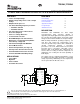
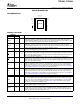
TPS54283,, TPS54286 www.ti.com SLUS749C – JULY 2007 – REVISED OCTOBER 2007 2-A DUAL NON-SYNCHRONOUS CONVERTER WITH INTEGRATED HIGH-SIDE MOSFET FEATURES CONTENTS 1 • 4.5-V to 28-V Input Range • Output Voltage Range 0.8 V to 90% of Input Voltage • Output Current Up to 2 A • Two Fixed Switching Frequency Versions: – TPS54283: 300 kHz – TPS54286: 600 kHz • Two Selectable Levels of Overcurrent Protection (Output 2) • 0.8-V 1.5% Voltage Reference • 2.
TPS54283,, TPS54286 www.ti.com SLUS749C – JULY 2007 – REVISED OCTOBER 2007 These devices have limited built-in ESD protection. The leads should be shorted together or the device placed in conductive foam during storage or handling to prevent electrostatic damage to the MOS gates.
TPS54283,, TPS54286 www.ti.com SLUS749C – JULY 2007 – REVISED OCTOBER 2007 ELECTRICAL CHARACTERISTICS –40°C ≤ TJ ≤ +125°C, VPVDD1 = VPVDD2 = 12 V, unless otherwise noted. PARAMETER TEST CONDITIONS MIN TYP MAX UNIT INPUT SUPPLY (PVDD) VPVDD1 VPVDD2 Input voltage range 4.5 28 V µA IDDSDN Shutdown VEN1 = VEN2 = VPVDD2 70 150 IDDQ Quiescent, non-switching VFB = 0.9V, Outputs off 1.8 3.
TPS54283,, TPS54286 www.ti.com SLUS749C – JULY 2007 – REVISED OCTOBER 2007 ELECTRICAL CHARACTERISTICS (continued) –40°C ≤ TJ ≤ +125°C, VPVDD1 = VPVDD2 = 12 V, unless otherwise noted.
TPS54283,, TPS54286 www.ti.com SLUS749C – JULY 2007 – REVISED OCTOBER 2007 TYPICAL CHARACTERISTICS QUIESCENT CURRENT (NON-SWITCHING) vs JUNCTION TEMPERATURE SHUTDOWN CURRENT vs JUNCTION TEMPERATURE 2.1 140 VBP = 5.25 V VPVDDx = 28 V 120 VPVDDx = 12 V ISD - Shutdown Current - mA IDDQ - Quiescent Current - mA 2.0 1.9 1.8 1.7 1.6 1.5 -50 100 80 60 40 VPVDDx = 4.
TPS54283,, TPS54286 www.ti.com SLUS749C – JULY 2007 – REVISED OCTOBER 2007 TYPICAL CHARACTERISTICS (continued) SOFT START TIME vs JUNCTION TEMPERATURE SWITCHING FREQUENCY (300 kHz) vs JUNCTION TEMPERATURE 3.5 350 VBP = 5.25 V fPWM - PWM Frequency - kHz tSS - Soft Start Time - ms VBP = 5.25 V 3.0 2.5 2.0 1.5 -50 -25 0 25 50 75 100 330 310 290 270 -50 125 -25 0 25 50 75 TJ - Junction Temperature - °C TJ - Junction Temperature - °C Figure 5. Figure 6.
TPS54283,, TPS54286 www.ti.com SLUS749C – JULY 2007 – REVISED OCTOBER 2007 TYPICAL CHARACTERISTICS (continued) FEEDBACK VOLTAGE vs JUNCTION TEMPERATURE OVERCURRENT LIMIT (CH1, CH2 HIGH LEVEL) vs JUNCTION TEMPERATURE 3.4 808 803 ICL - Overcurrent Limit - A VFB - Feedback Voltage - mV VPVDDx = 24 V 798 793 3.2 3.0 2.8 VPVDDx = 12 V VPVDDx = 5 V 788 -50 0 -25 25 50 75 100 2.6 -50 125 -25 0 25 50 75 100 TJ - Junction Temperature - °C TJ - Junction Temperature - °C Figure 9.
TPS54283,, TPS54286 www.ti.com SLUS749C – JULY 2007 – REVISED OCTOBER 2007 TYPICAL CHARACTERISTICS (continued) OVERCURRENT LIMIT vs SUPPLY VOLTAGE MINIMUM CONTROLLABLE PULSE WIDTH vs LOAD CURRENT OCL = 3.0 A 3.5 IOC - Overcurrent Limit - A tON - Minimum Controllable Pulse Width - ns 400 3.0 2.5 2.0 OCL = 1.5 A 1.5 TA(°C) TA = –40°C 300 250 TA = 0°C 200 150 TA = 25°C 100 TA = 85°C 1.0 4 8 12 16 20 VDD - Supply Voltage - V 24 28 50 0 0.2 Figure 13. 8 –40 0 25 85 350 0.4 0.6 0.
TPS54283,, TPS54286 www.ti.com SLUS749C – JULY 2007 – REVISED OCTOBER 2007 DEVICE INFORMATION PIN CONNECTIONS HTSSOP (PWP) (Top View) PVDD1 1 14 PVDD2 BOOT1 2 13 BOOT2 SW1 3 GND 4 EN1 5 10 SEQ EN2 6 9 ILIM2 FB1 7 8 FB2 12 SW2 Thermal Pad (bottom side) 11 BP TERMINAL FUNCTIONS TERMINAL I/O DESCRIPTION NAME NO. BOOT1 2 I Input supply to the high side gate driver for Output 1. Connect a 22-nF to 82-nF capacitor from this pin to SW1.
TPS54283,, TPS54286 www.ti.com SLUS749C – JULY 2007 – REVISED OCTOBER 2007 TERMINAL FUNCTIONS (continued) TERMINAL NAME NO. I/O DESCRIPTION SEQ 10 I This pin configures the output startup mode. If the SEQ pin is connected to BP, then when Output 2 is enabled, Output 1 is allowed to start after Output 2 has reached regulation; that is, sequential startup where Output 1 is slave to Output 2.
TPS54283,, TPS54286 www.ti.com SLUS749C – JULY 2007 – REVISED OCTOBER 2007 BLOCK DIAGRAM 2 BOOT1 1 PVDD1 3 SW1 BP CLK1 Level Shift Current Comparator f(IDRAIN1) + DC(ofst) + GND 4 + FB1 S Q R R Q f(IDRAIN1) 7 Overcurrent Comp + 0.8 VREF RCOMP Soft Start 1 SD1 f(ISLOPE1) BP f(IMAX1) CLK1 CCOMP Anti-Cross Conduction VDD2 Weak Pull-Down MOSFET f(ISLOPE1) Ramp Gen 1 TSD 6 mA EN1 5 EN2 6 1.
TPS54283,, TPS54286 www.ti.com SLUS749C – JULY 2007 – REVISED OCTOBER 2007 APPLICATION INFORMATION FUNCTIONAL DESCRIPTION The TPS54283 and TPS54286 are dual output non-synchronous converters. Each PWM channel contains an internally-compensated error amplifier, current mode pulse width modulator (PWM), switch MOSFET, enable, and fault protection circuitry. Common to the two channels are the internal voltage regulator, voltage reference, clock oscillator, and output voltage sequencing functions.
TPS54283,, TPS54286 www.ti.com SLUS749C – JULY 2007 – REVISED OCTOBER 2007 An R-C connected to an ENx pin may be used to delay the turn-on of the associated output after power is applied to PVDDx (see Figure 15). After power is applied to PVDD2, the voltage on the ENx pin slowly decays towards ground. Once the voltage decays to approximately 1.2 V, then the output is enabled and the startup sequence begins.
TPS54283,, TPS54286 www.ti.com SLUS749C – JULY 2007 – REVISED OCTOBER 2007 Output Voltage Sequencing The TPS5428x allows single-pin programming of output voltage startup sequencing. During power-on, the state of the SEQ pin is detected. Based on whether the pin is tied to BP, to GND, or left floating, the outputs behave as described in Table 1. Table 1.
TPS54283,, TPS54286 www.ti.com SLUS749C – JULY 2007 – REVISED OCTOBER 2007 DESIGN HINT An R-C network connected to the ENx pin may be used in addition to the SEQ pin in sequential mode to delay the startup of the first output voltage. This approach may be necessary in systems with a large number of output voltages and elaborate voltage sequencing requirements. See Enable and Timed Turn On of the Outputs.
TPS54283,, TPS54286 www.ti.com SLUS749C – JULY 2007 – REVISED OCTOBER 2007 to support the desired regulation voltage by the time Soft Start has completed, then the output UV circuit may trip and cause a hiccup in the output voltage. In this case, use a timed delay startup from the ENx pin to delay the startup of the output until the PVDDx voltage has the capability of supporting the desired regulation voltage. See Operating Near Maximum Duty Cycleand Maximum Output Capacitance for related information.
TPS54283,, TPS54286 www.ti.com SLUS749C – JULY 2007 – REVISED OCTOBER 2007 Feedback Loop and Inductor-Capacitor (L-C) Filter Selection In the feedback signal path, the output voltage setting divider is followed by an internal gM-type error amplifier with a typical transconductance of 30 µS. An internal series connected R-C circuit from the gM amplifier output to ground serves as the compensation network for the converter.
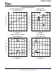
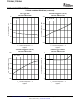
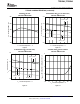
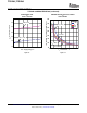
TPS54283,, TPS54286 www.ti.com SLUS749C – JULY 2007 – REVISED OCTOBER 2007 VIN VC + VOUT + Modulator VREF _ _ Filter Current Feedback Network Compensation Network Figure 22. Small Signal Equivalent Block Diagram Inductor-Capacitor (L-C) Selection The following figures plot the TPS5428x Output-to-Vc gain and phase versus frequency for various duty cycles (10%, 30%, 50%, 70%, 90%) at three (200 mA, 400 mA, 600 mA) peak-to-peak ripple current levels.
TPS54283,, TPS54286 www.ti.com SLUS749C – JULY 2007 – REVISED OCTOBER 2007 GAIN AND PHASE vs FREQUENCY 270 85 225 180 70 180 135 55 135 40 90 90 40 Gain - dB 225 45 25 20 0 10 0 -45 -20 100 1k 10 k 100 k f - Frequency -Hz -5 -90 1M -20 100 Figure 25.
TPS54283,, TPS54286 www.ti.com SLUS749C – JULY 2007 – REVISED OCTOBER 2007 R1 VREF (1 + R2 ) ´ TS tSS R1 1 + ) COUTmax = ICLx - VREF (1 + R2 ) (1 RLOAD VREF 2 ´ VIN ´ L (3) Minimum Output Capacitance Ensure the value of capacitance selected for closed loop stability is compatible with the requirements of Soft Start. Modifying The Feedback Loop Within the limits of the internal compensation, there is flexibility in the selection of the inductor and output capacitor values.
TPS54283,, TPS54286 www.ti.com SLUS749C – JULY 2007 – REVISED OCTOBER 2007 The value of the resistor is calculated using a ratio of impedances to match the ratio of ESR zero frequency to the desired zero frequency. R2 R3 = æ æ fZERO(desired) çç ç ç fESR(zero) èè ö ö ÷ - 1÷ ÷ ÷ ø ø (4) where • • fESR(zero) is the ESR zero frequency of the output capacitor fZERO(desired) is the desired frequency of the zero added to the feedback.
TPS54283,, TPS54286 www.ti.
TPS54283,, TPS54286 www.ti.com SLUS749C – JULY 2007 – REVISED OCTOBER 2007 Example: TPS54286 Buck Converter Operating at 12-V Input, 3.3-V Output and 400-mAp-p Ripple Current First, the steady state duty cycle is calculated. Assuming the rectifier diode has a voltage drop of 0.5 V, the duty cycle is approximated using Equation 10. VOUT + VDIODE 3.3 + 0.5 = 30% d= = VIN + VDIODE 12 + 0.5 (10) The filter inductor is then calculated; see Equation 11. V - VOUT 12 - 3.3 1 ´ d ´ TS = ´ 0.3 ´ = 10.
TPS54283,, TPS54286 www.ti.com SLUS749C – JULY 2007 – REVISED OCTOBER 2007 Bootstrap for the N-Channel MOSFET A bootstrap circuit provides a voltage source higher than the input voltage and of sufficient energy to fully enhance the switching MOSFET each switching cycle. The PWM duty cycle is limited to a maximum of 90%, allowing an external bootstrap capacitor to charge through an internal synchronous switch (between BP and BOOTx) during every cycle.
TPS54283,, TPS54286 www.ti.com SLUS749C – JULY 2007 – REVISED OCTOBER 2007 SW Waveform SW Waveform VOUT Ripple VOUT Ripple Skipping VIN = 12 V VOUT = 5 V Inductor Current Steady State VIN = 12 V VOUT = 5 V Inductor Current Figure 31. Steady State Figure 32.
TPS54283,, TPS54286 www.ti.com SLUS749C – JULY 2007 – REVISED OCTOBER 2007 Output Overload Protection In the event of an overcurrent during soft start on either output (such as starting into an output short), pulse-by-pulse current limiting and PWM frequency division (see below) are in effect for that output until the internal soft start timer ends. At the end of the soft start time, a UV condition is declared and a fault is declared.
TPS54283,, TPS54286 www.ti.com SLUS749C – JULY 2007 – REVISED OCTOBER 2007 The preferred sequence of events is: 1. PVDD2 rises above the input UVLO voltage 2. PVDD1 rises with Output 1 disabled until PVDD1 rises above level to support Output 1 regulation. With these two conditions satisfied, there is no restriction on PVDD2 to be greater than, or less than PVDD1.
TPS54283,, TPS54286 www.ti.com SLUS749C – JULY 2007 – REVISED OCTOBER 2007 PVDD2 Output2 PVDD1 Output1 T - Time Figure 34. Waveforms Resulting from Cascading PVDD1 from Output 2 In this configuration, the following conditions must be maintained: 1. Output 2 must be of a voltage high enough to maintain regulation of Output 1 under all load conditions. 2. The sum of the current drawn by Output 2 load plus the current into PVDD1 must be less than the overload protection current level of Output 2. 3.
TPS54283,, TPS54286 www.ti.com SLUS749C – JULY 2007 – REVISED OCTOBER 2007 2 æ æ (D I 2 OUTPUTx ) IRMS(outputx) = D ´ ç (IOUTPUTx ) + ç çç ç 12 è è öö ÷÷ ÷ ÷÷ øø (16) where • • • D is the duty cycle IOUTPUTx is the DC output current ΔIOUTPUTx is the peak ripple current in the inductor for Outputx Notice the impact of the operating duty cycle on the result. Multiplying the result by the RDS(on) of the MOSFET gives the conduction loss.
TPS54283,, TPS54286 www.ti.com SLUS749C – JULY 2007 – REVISED OCTOBER 2007 POWER DISSIPATION vs AMBIENT TEMPERATURE 1.8 LFM = 250 1.6 LFM = 500 PD - Power Dissipation - W 1.4 LFM = 0 1.2 LFM = 150 1.0 0.8 0.6 LFM 0 150 250 500 0.4 0.2 0 0 20 40 60 80 100 120 TA - Ambient Temperature - °C 140 Figure 35.
TPS54283,, TPS54286 www.ti.com SLUS749C – JULY 2007 – REVISED OCTOBER 2007 PowerPAD Package The PowerPAD package provides low thermal impedance for heat removal from the device. The PowerPAD derives its name and low thermal impedance from the large bonding pad on the bottom of the device. The circuit board must have an area of solder-tinned-copper underneath the package. The dimensions of this area depend on the size of the PowerPAD package.
TPS54283,, TPS54286 www.ti.com SLUS749C – JULY 2007 – REVISED OCTOBER 2007 L2 C18 R8 C14 C17 R6 C13 D2 C19 VOUT2 GND C15 R7 R4 R9 C16 C8 C12 C11 C6 U1 1 VIN R2 C10 R5 C1 D1 GND C7 C3 C4 C9 GND C5 R3 VOUT1 L1 Figure 36. Top Layer Copper Layout and Component Placement Figure 37.
TPS54283,, TPS54286 www.ti.com SLUS749C – JULY 2007 – REVISED OCTOBER 2007 DESIGN EXAMPLES Example 1: Detailed Design of a 12-V to 5-V and 3.3-V Converter The following example illustrates a design process and component selection for a 12-V to 5-V and 3.3-V dual non-synchronous buck regulator using the TPS54283 converter. Design Example List of Materials and Table 4, Definition of Symbols is found at the end of this section. PARAMETER NOTES AND CONDITIONS MIN NOM MAX UNIT 6.
TPS54283,, TPS54286 www.ti.com SLUS749C – JULY 2007 – REVISED OCTOBER 2007 Design Procedure Duty Cycle Estimation The first step is to estimate the duty cycle of each switching FET. VOUT + VFD VIN(min) + VFD Dmax » Dmin » (21) VOUT + VFD VIN(max) + VFD (22) Using an assumed forward drop of 0.5 V for a schottky rectifier diode, the Channel 1 duty cycle is approximately 40.1% (minimum) to 48.7% (maximum) while the Channel 2 duty cycle is approximately 27.7% (minimum) to 32.2% (maximum).
TPS54283,, TPS54286 www.ti.com SLUS749C – JULY 2007 – REVISED OCTOBER 2007 V(BR )R(min ) ³ 1.2 ´ VIN (27) The diode must have reverse breakdown voltage greater than 15.8 V, therefore a 20-V device is used. The average current in the rectifier diode is estimated by Equation 28. ID(avg) » IOUT(max ) ´ (1 - D ) (28) For this design, 1.2-A (average) and 2.25 A (peak) is estimated for Channel 1 and 1.5-A (average) and 2.21-A (peak) for Channel 2.
TPS54283,, TPS54286 www.ti.com SLUS749C – JULY 2007 – REVISED OCTOBER 2007 Voltage Setting The primary feedback divider resistors (R2, R9) from VOUT to FB should be between 10 kΩ and 50 kΩ to maintain a balance between power dissipation and noise sensitivity. For this design, 20 kΩ is selected. The lower resistors, R4 and R7 are found using the following equations. R4 = R7 = • • • • VFB ´ R2 VOUT1 - VFB (32) VFB ´ R9 VOUT2 - VFB (33) R2 = R9 = 20 kΩ VFB = 0.80 V R4= 3.80 kΩ (3.
TPS54283,, TPS54286 www.ti.com SLUS749C – JULY 2007 – REVISED OCTOBER 2007 Input Capacitor Selection The TPS54283 datasheet recommends a minimum 10-µF ceramic input capacitor on each PVDD pin. These capacitor must be capable of handling the RMS ripple current of the converter. The RMS current in the input capacitors is estimated by Equation 38. 2 æ æ (D I 2 OUTPUTx ) IRMS(outputx) = D ´ ç (IOUTPUTx ) + ç çç ç 12 è è • öö ÷÷ ÷ ÷÷ øø (38) IRMS(CIN) = 0.
TPS54283,, TPS54286 www.ti.com SLUS749C – JULY 2007 – REVISED OCTOBER 2007 PREG » IDD ´ VIN(max ) + IBP ´ VIN(max ) - VBP ( ) (42) With no external load on BP (IBP=0) the regulator power dissipation is 66 mW. Total power dissipation in the device is the sum of conduction and switching for both channels plus regulator losses. The total power dissipation is PDISS=0.198+0.136+0.017+0.017+.066 = 434 mW. Design Example Test Results The following results are from the TPS54283-001 EVM. VIN = 12 V SW 3.
TPS54283,, TPS54286 SLUS749C – JULY 2007 – REVISED OCTOBER 2007 1.005 1.005 1.004 1.004 VOUT - Output Voltage (Normalized) - V 1.003 VIN = 13.2 V 1.002 VIN = 12.0 V 1.001 1.000 0.999 VOUT = 5.0 V 0.998 VIN = 9.6 V 0.997 VIN (V) 0.996 9.6 12.0 13.2 1.003 1.002 All Input Voltages 1.001 1.000 0.999 0.998 0.997 0.996 0.995 0.995 0 0.4 0.8 1.2 1.6 2.0 0 0.4 0.8 1.2 1.6 2.0 IOUT - Load Current - A Figure 42. 5.0-V Output Voltage vs. Load Current Figure 43. 3.3-V Output Voltage vs.
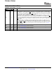
TPS54283,, TPS54286 www.ti.com SLUS749C – JULY 2007 – REVISED OCTOBER 2007 Table 3. Design Example List of Materials QTY 40 REFERENCE DESIGNATOR VALUE DESCRIPTION SIZE PART NUMBER MANUFACTURER 1 C1 100 µF Capacitor, Aluminum, 25V, E-can EEEFC1E101P Panasonic 2 C10, C11 10 µF Capacitor, Ceramic, 25V, X5R 20% 1210 C3216X5R1E106M TDK 1 C12 4.7 µF Capacitor, Ceramic, 10V, X5R 20% 0805 Std Std 2 C14, C16 470 pF Capacitor, Ceramic, 25V, X7R, 20% 0603 Std Std 1 C15 6.
TPS54283,, TPS54286 www.ti.com SLUS749C – JULY 2007 – REVISED OCTOBER 2007 Table 4.
TPS54283,, TPS54286 www.ti.com SLUS749C – JULY 2007 – REVISED OCTOBER 2007 Additional Design Examples Example 2: 24-V to 12-V and 24-V to 5-V For a higher input voltage, both a snubber and bootstrap resistors are added to reduce ringing on the switch node and a 30 V schottky diode is selected. A higher resistance feedback network is chosen for the 12 V output to reduce the feedback current. + + Figure 45.
TPS54283,, TPS54286 www.ti.com SLUS749C – JULY 2007 – REVISED OCTOBER 2007 90 80 VOUT = 12 V h - Efficiency - % 70 VOUT = 5 V 60 50 40 VIN = 24 V 30 VOUT (V) 20 5 12 10 0 0 0.5 1.0 1.5 IOUT - Load Current - A 2.0 2.5 Figure 48. Efficiency vs.
TPS54283,, TPS54286 www.ti.com SLUS749C – JULY 2007 – REVISED OCTOBER 2007 Example 3: 5-V to 3.3V and 5-V to 1.2 V For a low input voltage application, the TPS54286 is selected for reduced size and all ceramic output capacitors are used. 22-µF input capacitors are selected to reduce input ripple and lead capacitors are placed in the feedback to boost phase margin. Figure 49. 5-V to 3.3V and 5-V to 1.2 V 80 100 80 70 VOUT = 3.3 V Gain - dB VOUT = 1.
TPS54283,, TPS54286 www.ti.com SLUS749C – JULY 2007 – REVISED OCTOBER 2007 ADDITIONAL REFERENCES Related Devices The following parts have characteristics similar to the TPS54283/6 and may be of interest. Table 5. Devices Related to the TPS54283 and TPS54286 TI LITERATURE NUMBER DEVICE SLUS642 TPS40222 5-V Input, 1.
PACKAGE OPTION ADDENDUM www.ti.
PACKAGE OPTION ADDENDUM www.ti.com 11-Apr-2013 (4) Multiple Top-Side Markings will be inside parentheses. Only one Top-Side Marking contained in parentheses and separated by a "~" will appear on a device. If a line is indented then it is a continuation of the previous line and the two combined represent the entire Top-Side Marking for that device. Important Information and Disclaimer:The information provided on this page represents TI's knowledge and belief as of the date that it is provided.
IMPORTANT NOTICE Texas Instruments Incorporated and its subsidiaries (TI) reserve the right to make corrections, enhancements, improvements and other changes to its semiconductor products and services per JESD46, latest issue, and to discontinue any product or service per JESD48, latest issue. Buyers should obtain the latest relevant information before placing orders and should verify that such information is current and complete.