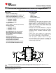
TPS54290, TPS54291, TPS54292 www.ti.com SLUS973 – OCTOBER 2009 1.5-A/2.5-A Dual, Fully-Synchronous Buck Converter With Integrated MOSFET Check for Samples :TPS54290 TPS54291 TPS54292 FEATURES APPLICATIONS • • • • • • • • 1 2 • • • • • • • • • • • 4.5 V to 18 V Input Range Output Voltage Range 0.8 V to DMAX × VIN Fully Integrated Dual Buck, 1.5 A/2.5 A Three Fixed Switching Frequency Versions: – TPS54290 – 300 kHz – TPS54291 – 600 kHz – TPS54292 – 1.2 MHz Integrated UVLO 0.
TPS54290, TPS54291, TPS54292 SLUS973 – OCTOBER 2009 www.ti.com This integrated circuit can be damaged by ESD. Texas Instruments recommends that all integrated circuits be handled with appropriate precautions. Failure to observe proper handling and installation procedures can cause damage. ESD damage can range from subtle performance degradation to complete device failure.
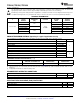
TPS54290, TPS54291, TPS54292 www.ti.com SLUS973 – OCTOBER 2009 ELECTRICAL CHARACTERISTICS TJ = –40°C to 125°C, PVDD1 and 2 = 12V (unless otherwise noted) PARAMETER TEST CONDITIONS MIN TYP MAX UNIT INPUT SUPPLY PVDD1, PVDD2 Input voltage range 18 V IDDSDN Shutdown current EN1=EN2 = PVDD2 (4.5-18V) 80 160 µA IDDQ Quiescent, non-switching FB1 = FB2 = 1 V, Outputs Off 1.65 3.00 mA IDDSW Quiescent, while switching FB1 = FB2 = 0.
TPS54290, TPS54291, TPS54292 SLUS973 – OCTOBER 2009 www.ti.
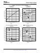
TPS54290, TPS54291, TPS54292 www.ti.com SLUS973 – OCTOBER 2009 TYPICAL PERFORMANCE CHARACTERISTICS QUIESCENT CURRENT vs TEMPERATURE SHUTDOWN CURRENT vs TEMPERATURE 1.75 140 Non-Switching 120 ISD – Shutdown Current – mA IDDQ – Quiescent Current – mA 1.70 1.65 1.60 VIN = 18 V 100 80 VIN = 12 V 60 40 1.55 VIN = 4.5 V 20 0 –40 –25 –10 5 20 35 50 65 80 95 110 125 TJ – Junction Temperature – °C Figure 1. Figure 2.
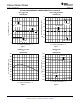
TPS54290, TPS54291, TPS54292 SLUS973 – OCTOBER 2009 www.ti.com TYPICAL PERFORMANCE CHARACTERISTICS (continued) SOFT START TIME vs TEMPERATURE OSCILLATOR FREQUENCY vs TEMPERATURE 1.4 6 tSS – Soft-Start Time – ms 4 fSW = 300 kHz fSW = 600 kHz 3 2 fSW – Switching Frequency – MHz 1.2 5 1 fSW = 1.2 MHz fSW = 600 kHz 0.8 0.6 0.4 0.2 fSW = 300 kHz 0 –40 –25 –10 5 20 35 50 65 80 95 110 125 TJ – Junction Temperature – °C fSW = 1.
TPS54290, TPS54291, TPS54292 www.ti.com SLUS973 – OCTOBER 2009 TYPICAL PERFORMANCE CHARACTERISTICS (continued) BP VOLTAGE vs TEMPERARURE SW NODE LEAKAGE CURRENT vs TEMPERATURE 5.20 9 VBP – BP Regulation Voltage – V ISW(off) – Switch-Node Current – mA 8 5.15 5.10 5.05 VVDD = 12 V 5.00 –40 –25 –10 5 20 35 50 65 80 95 110 125 TJ – Junction Temperature – °C 7 6 5 4 3 2 1 0 -1 –40 –25 –10 5 20 35 50 65 80 95 110 125 TJ – Junction Temperature – °C Figure 9. Figure 10.
TPS54290, TPS54291, TPS54292 SLUS973 – OCTOBER 2009 www.ti.com DEVICE INFORMATION HTSSOP (PWP) (Top View) PVDD1 1 16 PVDD2 BOOT1 2 15 BOOT2 SW1 3 14 SW2 PGND1 4 13 PGND2 EN1 5 12 BP EN2 6 11 GND FB1 7 COMP1 8 10 FB2 Thermal Pad (bottom side) 9 COMP2 PIN FUNCTIONS PIN NAME NO. BOOT1 2 I/O DESCRIPTION I Input supply to the high-side gate driver for Output1. Connect a 22 nF to 68 nF capacitor from this pin to SW1.
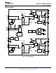
TPS54290, TPS54291, TPS54292 www.ti.com SLUS973 – OCTOBER 2009 BLOCK DIAGRAM BP f(IDRAIN1) + DC(ofst) Current Comparator FET Switch CLK1 + COMP1 8 f(IDRAIN1) FB1 + R R Q 1 PVDD1 IDRAIN1 3 SW1 4 PGND1 BP Overcurrent Comp f(ISLOPE1) Soft Start 1 Q BOOT1 + 7 0.8 VREF S 2 f(IMAX1) CLK1 Anti-Cross Conduction SD1 TSD 10 mA (max) EN1 EN2 10 mA (max) 5 SD1 Internal Control 6 f(ISLOPE1) Ramp Gen 1 SD2 UVLO FB1 FB2 2.
TPS54290, TPS54291, TPS54292 SLUS973 – OCTOBER 2009 www.ti.com APPLICATION INFORMATION FUNCTIONAL DESCRIPTION The TPS54290/1/2 is a dual output fully synchronous buck converter. Each PWM channel contains an error amplifier, current mode pulse width modulator (PWM), switching and rectifying MOSFETs, enable, and fault protection circuitry. Common to the two channels are the internal voltage regulator, voltage reference, and clock oscillator.
X TPS54290, TPS54291, TPS54292 www.ti.com SLUS973 – OCTOBER 2009 PVDD2 10 mA (max) ENx C + PVDDx R PVDDx 1.25 V 1.25-V Threshold TPS5429x UDG-09125 ENxB VOUTx Time 0 Figure 12. Startup Delay Schematic tDELAY tDELAY + tSS Figure 13. Startup Delay Timing Diagram NOTE If delayed output voltage startup is not necessary, simply connect EN1 and EN2 to GND. This allows the outputs to “start” immediately on the valid application of PVDD2.
TPS54290, TPS54291, TPS54292 SLUS973 – OCTOBER 2009 www.ti.com OUTPUT VOLTAGE REGULATION The regulation output voltage is determined by a resistor divider connecting the output node, the FBx pin, and GND (Figure 14). The value of the output voltage is shown in Equation 2. R1 ö æ VOUT = VREF ´ ç 1 + ÷ (V ) è R2 ø (2) where • VREF is the internal 0.
TPS54290, TPS54291, TPS54292 www.ti.com SLUS973 – OCTOBER 2009 MAXIMUM OUTPUT CAPACITANCE With internal pulse-by-pulse current limiting and a fixed soft-start time, there is a maximum output capacitance which may be used before startup problems begin to occur. If the output capacitance is large enough so that the device enters a current-limit protection mode during startup, then there is a possibility that the output never reaches regulation.
TPS54290, TPS54291, TPS54292 SLUS973 – OCTOBER 2009 www.ti.com V IN VREF VC + VOUT + Modulator _ _ Filter Current Feedback Network Compensation Network Figure 16. Small Signal Equivalent Block Diagram To determine the components necessary for compensating the feedback loop, the controller frequency response characteristics must be understood and the desired crossover frequency selected.
TPS54290, TPS54291, TPS54292 www.ti.com SLUS973 – OCTOBER 2009 TPS54290 VOUT1 ZUPPER C1 (Optional) C2 (Optional) R1 R2 1 PVDD1 PVDD2 16 2 BOOT1 BOOT2 15 3 SW1 4 PGND1 5 EN1 BP 12 6 EN2 GND 11 7 FB1 FB2 10 8 COMP1 SW2 14 PGND2 13 COMP2 9 RCOMP CCOMP ZLOWER UDG-09129 Figure 17. Loop Compensation Network If operating at wide duty cycles (over 50%), a capacitor may be necessary across the upper resistor of the voltage setting divider.
TPS54290, TPS54291, TPS54292 SLUS973 – OCTOBER 2009 www.ti.com BOOTSTRAP FOR N-CHANNEL MOSFET A bootstrap circuit provides a voltage source higher than the input voltage and of sufficient energy to fully enhance the switching MOSFET each switching cycle. The PWM duty cycle is limited to maximum, i.e., 90% for TPS54291, allowing an external bootstrap capacitor to charge through an internal synchronous switch (between BP and BOOTx) during every cycle.
TPS54290, TPS54291, TPS54292 www.ti.com SLUS973 – OCTOBER 2009 OVER-TEMPERATURE PROTECTION AND JUNCTION TEMPERATURE RISE The over temperature thermal protection limits the maximum power to be dissipated at a given operating ambient temperature. In other words, at a given device power dissipation, the maximum ambient operating temperature is limited by the maximum allowable junction operating temperature.
TPS54290, TPS54291, TPS54292 SLUS973 – OCTOBER 2009 www.ti.com POWER DERATING The TPS5429x delivers full current at wide duty cycles at ambient temperatures up to 85°C if the thermal impedance from the thermal pad is sufficient to maintain the junction temperature below the thermal shut down level. At higher ambient temperatures, the device power dissipation must be reduced to maintain the junction temperature at or below the thermal shutdown level.
TPS54290, TPS54291, TPS54292 www.ti.com SLUS973 – OCTOBER 2009 LAYOUT RECOMMENDATIONS • • • • • • • • • • The PowerPad must be connected to the low-current ground with available surface copper to dissipate heat. Extending ground land beyond the device package area between PVDD1 (pin 1) and PVDD2 (pin 16) and between COMP1 (pin 8) and COMP2( pin 9) is recommended.. Connect PGND1 and PGND2 to the PowerPad through a 10-mil wide trace.
TPS54290, TPS54291, TPS54292 SLUS973 – OCTOBER 2009 www.ti.com DESIGN EXAMPLES Design Example 1 The following example illustrates the design process and component selection for a 12-V to 5-V and 3.3-V dual non-synchronous buck regulator using the TPS54291 converter. A definition of symbols used can be found in Table 1 of the appendix Table 1. Design Example Electrical Characteristics PARAMETER TEST CONDITIONS MIN TYP MAX UNIT 8 12 14 V 12 20 mA 4.2 4.
TPS54290, TPS54291, TPS54292 www.ti.com SLUS973 – OCTOBER 2009 The list of materials for this application is shown below in Table 2. The efficiency, line regulation and load regulation from printed circuit boards built using this design are shown in Figure 23 and Figure 24. Figure 21. TPS54291 Design Example 1 Schematic Step by Step Design Procedure Duty Cycle Estimation The duty cycle of the main switching FET is estimated by Equation 16 and Equation 17. DMAX1 » VOUT VOUT 3.3 1.2 = = 0.
TPS54290, TPS54291, TPS54292 SLUS973 – OCTOBER 2009 IRIPPLE1 » IRIPPLE2 » www.ti.com VIN(max ) - VOUT L1 VIN(max ) - VOUT L2 ´ DMIN ´ ´ DMIN ´ 1 fSW 1 fSW = = 14 - 3.3 1 ´ 0.236 ´ = 0.513 A 8.2 mH 600kHz (22) 14 - 1.2 1 ´ 0.086 ´ = 0.556A 3.3 mH 600kHz (23) The RMS current through the inductor is approximated by Equation 24 and Equation 25. IL(rms ) = IL(avg)2 + 2 1 I 12 RIPPLE » IOUT(max )2 + 2 1 I 12 RIPPLE = (1.5 )2 + 112 (0.513 )2 A = 1.
TPS54290, TPS54291, TPS54292 www.ti.com SLUS973 – OCTOBER 2009 IRMS(CIN1) = IOUT1 ´ D1 ´ (1 - D1 ) = 1.5 A ´ 0.413 ´ (1 - 0.413 ) = 0.74 A (32) IRMS(CIN2 ) = IOUT1 ´ D2 ´ (1 - D2 ) = 2.5 A ´ 0.15 ´ (1 - 0.15 ) = 0.89 A (33) One 1210 10-µF, 25-V, X5R, ceramic capacitor with 2-mΩ ESR and a 2-A RMS current rating are selected for each PVDD input.
TPS54290, TPS54291, TPS54292 SLUS973 – OCTOBER 2009 www.ti.com Compensation Gain Setting Resistor RCOMP programs the mid-band error amplifier gain to set the desired cross-over frequency in Equation 38. RCOMP = 10 KEA 20 ´ (ZLOWER + ZUPPER ) 10 = gM ´ ZLOWER 11.83dB 20 ´ (6.49kW + 20.5kW) = 50.42kW » 53.6kW 325 mS ´ 6.
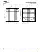
TPS54290, TPS54291, TPS54292 www.ti.com SLUS973 – OCTOBER 2009 Design Example Test Results Figure 22. TPS54291 Design Example Switching Waveforms 90 100 VIN = 8 V 85 VIN = 8 V 95 90 80 h – Efficiency – % h – Efficiency – % 85 VIN = 12 V 75 70 VIN = 14 V 65 VIN = 14 V 80 75 VIN = 12 V 70 65 60 60 55 VOUT = 1.2 V 50 55 VOUT = 3.3 V 50 0 0.5 1.0 1.5 2.0 ILOAD – Load Current – A Figure 23. Design Efficiency for 1.2-V Output 2.5 0 0.3 0.6 0.9 1.2 ILOAD – Load Current – A 1.
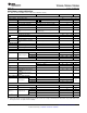
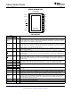
TPS54290, TPS54291, TPS54292 SLUS973 – OCTOBER 2009 www.ti.com Table 2. Design Example List of Materials REFERENCE DESIGNATOR QTY VALUE DESCRIPTION SIZE PART NUMBER MFR C12 1 4.7 µF Capacitor, Ceramic, 10 V, X5R, 20% 0805 Std C2, C14 2 22 µF Capacitor, Ceramic, 6.3 V, X5R, 20% 1206 C3216X5R0J226M TDK Std C3, C13 2 470 pF Capacitor, Ceramic, 25 V, X7R, 20% 0603 Std Std C4, C11 2 0.
TPS54290, TPS54291, TPS54292 www.ti.com SLUS973 – OCTOBER 2009 Design Example 2 (Cascading Operation) TPS5429x can be configured as cascaded operation as shown in Figure 25. The 12-V input supply is applied to PVDD2 and the the channel 2 output is tied to PVDD1. The channel 2 output is 3.3 V and capable of supporting 1.5 A to the load while generating power for the 1.2-V input for channel 1. + + 3.3V@1.5A 1.2V@1.5A + + Figure 25.
TPS54290, TPS54291, TPS54292 SLUS973 – OCTOBER 2009 www.ti.com ADDITIONAL REFERENCES RELATED DEVICES The following devices have characteristics similar to the TPS54290/1/2 and may be of interest. DEVICE DESCRIPTION TPS40222 5-V input, 1.
PACKAGE OPTION ADDENDUM www.ti.
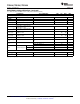
PACKAGE MATERIALS INFORMATION www.ti.com 14-Dec-2012 TAPE AND REEL INFORMATION *All dimensions are nominal Device Package Package Pins Type Drawing SPQ Reel Reel A0 Diameter Width (mm) (mm) W1 (mm) B0 (mm) K0 (mm) P1 (mm) TPS54290PWPR HTSSOP PWP 16 2000 330.0 12.4 TPS54291PWPR HTSSOP PWP 16 2000 330.0 TPS54292PWPR HTSSOP PWP 16 2000 330.0 6.9 5.6 1.6 8.0 12.0 Q1 12.4 6.9 5.6 1.6 8.0 12.0 Q1 12.4 6.9 5.6 1.6 8.0 12.
PACKAGE MATERIALS INFORMATION www.ti.com 14-Dec-2012 *All dimensions are nominal Device Package Type Package Drawing Pins SPQ Length (mm) Width (mm) Height (mm) TPS54290PWPR HTSSOP PWP 16 2000 367.0 367.0 35.0 TPS54291PWPR HTSSOP PWP 16 2000 367.0 367.0 35.0 TPS54292PWPR HTSSOP PWP 16 2000 367.0 367.0 35.
IMPORTANT NOTICE Texas Instruments Incorporated and its subsidiaries (TI) reserve the right to make corrections, enhancements, improvements and other changes to its semiconductor products and services per JESD46, latest issue, and to discontinue any product or service per JESD48, latest issue. Buyers should obtain the latest relevant information before placing orders and should verify that such information is current and complete.