
Datasheet


www.ti.com
Introduction
1 Introduction
The TPS542951 is a dual, adaptive on-time, D-CAP2™-mode, synchronous buck converter requiring a
low, external component count. The D-CAP2 control circuit is optimized for low-ESR output capacitors
such as POSCAP, SP-CAP, or ceramic types and features fast transient response with no external
compensation. The switching frequency is internally set at a nominal of 700 kHz. The high-side and low-
side switching MOSFETs are incorporated inside the TPS542951 package along with the gate drive
circuitry. The low, drain-to-source on-resistance of the MOSFETs allows the TPS542951 to achieve high
efficiencies and helps keep the junction temperature low at high-output currents. The TPS542951 also
features auto-skip Eco-mode™ operation for improved light-load efficiency. The TPS542951 dual DC/DC
synchronous converter is designed to provide up to 3 A output on CH1 and 3 A output on CH2 from an
input voltage source of 4.5 V to 18 V. The output voltage range is from 0.76 V to 7 V. Rated input voltage
and output current range for the evaluation module are given in Table 1.
The TPS542951 EVM evaluation module is a dual, synchronous buck converter providing 3.3 V at 2 A on
CH1 and 1.5 V at 3 A on CH2 from 5 V to 18 V input. This user’s guide describes the TPS542951 EVM
performance.
NOTE: Throughout the document, x means 1 or 2, for example, VFBx means VFB1 or VFB2.
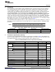
Table 1. Input Voltage, Output Voltage and Output Current Summary
TPS542951EVM Input Voltage Range Output Voltage Output Current Range
CH1 V
IN1
= 6 V to 18 V 3.3 V 0 A to 2 A
CH2 V
IN2
= 5 V to 18 V 1.5 V 0 A to 3 A
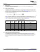
2 Performance Specification Summary
A summary of the TPS542951EVM performance specifications is provided in Table 2. Specifications are
given for an input voltage of V
INx
= 12 V and an output voltage of 3.3 V and 1.5 V, unless otherwise noted.
The ambient temperature is 25°C for all measurement, unless otherwise noted.
Table 2. TPS542951EVM Performance Specifications Summary
Specifications Test Conditions Min Typ Max Unit
Input voltage range (V
INx
)
(1)
12 18 V
V
OUT1
3.3
Output
V
voltages
V
OUT2
1.5
V
IN1
, V
IN2
= 12 V, I
OUT1
= 1 A, I
OUT2
= 700 kHz
Operating frequency
1.5 A
CH1 0 4 A
Output
current range
CH2 0 2
I
OUT1
= 1 A, I
OUT2
= 0 A, V
IN1
, V
IN2
= 6 V +0.25 , %
Line regulation, V
OUT1
to 18 V -0.55
I
OUT2
= 1.5 A, I
OUT1
= 0 A, V
IN1
, V
IN2
= 5 +0.15, %
Line regulation, V
OUT2
V to 18 V -0.35
+0.4, -
Load regulation, V
OUT1
V
IN1
, V
IN2
= 12 V, I
OUT1
= 0 A to 2 A %
0.1
+0.5, -
Load regulation, V
OUT2
V
IN1
, V
IN2
= 12 V, I
OUT2
= 0 A to 3 A %
0.05
Over current limit, V
OUT1
V
IN1
= 12 V, L
1
= 2.2 µH 2.7 3.9 4.5 A
Over current limit, V
OUT2
V
IN2
= 12 V, L
1
= 1.5 µH 3.5 4.7 5.4 A
Output ripple voltage, V
OUT1
V
IN1
= 12 V, I
OUT1
= 2 A 20 mV
PP
Output ripple voltage, V
OUT2
V
IN2
= 12 V, I
OUT2
= 3 A 20 mV
PP
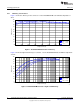
Maximum efficiency, V
OUT1
V
IN1
= 6 V, I
OUT1
= 0.6 A 94.1%
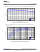
Maximum efficiency, V
OUT2
V
IN2
= 5 V, I
OUT2
= 0.5 A 88.8%
(1)
See Table 1
3
SLVU767–August 2012 TPS542951 Dual Channel SWIFT™ Evaluation Module
Submit Documentation Feedback
Copyright © 2012, Texas Instruments Incorporated