
Datasheet


www.ti.com
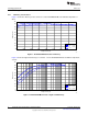
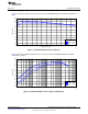
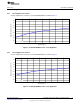
Test Setup and Results
4 Test Setup and Results
This section describes how to properly connect, set up, and use the TPS542951EVM. The section also
includes test results typical for the evaluation modules and efficiency, output load regulation, output line
regulation, load transient response, output voltage ripple, input voltage ripple, start-up, and switching
frequency.
4.1 Input/Output Connections
The TPS542951EVM is provided with input/output connectors and test points as shown in Table 4. A
power supply capable of supplying 4 A must be connected to J1 through a pair of 20 AWG wires. The
loads must be connected to J3 and/or J2 through a pair of 20 AWG wires. The maximum load current
capability is 2 times 2 A. Wire lengths must be minimized to reduce losses in the wires. Test point TP1
provides a place to monitor the input voltage (V
IN
) with TP7 providing a convenient ground reference. TP4
and TP3 are used to monitor the output voltages with TP5 and TP6 as the ground references.
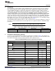
Table 4. Connection and Test Points
Reference Designator Function
J1 V
IN
(see Table 1 for V
IN
range)
J2 V
OUT2
, 1.5 V at 3 A maximum
J3 V
OUT1
, 3.3 V at 2 A maximum
J4 EN1 control. Connect EN1 to off to disable converter 1; connect EN1 to on to enable converter 1.
J5 EN2 control. Connect EN2 to off to disable converter 2; connect EN2 to on to enable converter 2.
JP1 Jumper to give the possibility to use another input voltage for converter 2.
TP1 V
IN
test point at V
IN
connector
TP2 V
IN2
test point after JP1.
TP3 Output voltage test point for converter 2.
TP4 Output voltage test point for converter 1.
TP5, TP6, TP7 Ground test points at input and output connectors.
TP8 EN2 test point.
TP9 EN1 test point.
TP10 Switch node test point of converter 1.
TP11 Switch node test point of converter 2.
TP12 VREG5 test point.
TP13 PG1 test point.
TP14 PG2 test point.
TP15 Analog ground test point.
4.2 Start-Up Procedure
1. Ensure that the jumper at J4 and/or J5 (Enable control) are set from ENx to off.
2. Apply appropriate V
IN
voltage to VIN and PGND terminals at J1.
3. Move the jumper at J4 and/or J5 (Enable control) to cover ENx and on. The EVM enables the
according output voltage.
5
SLVU767–August 2012 TPS542951 Dual Channel SWIFT™ Evaluation Module
Submit Documentation Feedback
Copyright © 2012, Texas Instruments Incorporated