
Datasheet

TPS54311, TPS54312
TPS54313, TPS54314
TPS54315, TPS54316
SLVS416B − FEBRUARY 2002 − REVISED APRIL 2005
www.ti.com
10
LAYOUT CONSIDERATIONS FOR THERMAL
PERFORMANCE
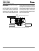
For operation at full rated load current, the analog ground
plane must provide adequate heat dissipating area. A 3
inch by 3 inch plane of 1 ounce copper is recommended,
though not mandatory, depending on ambient temperature
and airflow. Most applications have larger areas of internal
ground plane available, and the PowerPAD should be
connected to the largest area available. Additional areas
on the top or bottom layers also help dissipate heat, and
any area available should be used when 3 A or greater
operation is desired. Connection from the exposed area of
the PowerPAD to the analog ground plane layer should be
made using 0.013 inch diameter vias to avoid solder
wicking through the vias. Six vias should be in the
PowerPAD area with four additional vias located under the
device package. The size of the vias under the package,
but not in the exposed thermal pad area, can be increased
to 0.018. Additional vias beyond the ten recommended
that enhance thermal performance should be included in
areas not under the device package.
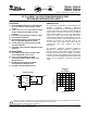
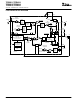
Minimum Recommended Exposed
Copper Area For Powerpad. 5mm
Stencils may Require 10 Percent
Larger Area
0.2454
0.0150
0.06
0.0256
0.1700
0.1340
0.0620
0.0400
0.0400
0.0400
0.0600
0.0227
0.0600
0.1010
6 PL ∅ 0.0130
4 PL ∅ 0.0180
Connect Pin 1 to Analog Ground Plane
in This Area for Optimum Performance
Minimum Recommended Top
Side Analog Ground Area
Minimum Recommended Thermal Vias: 6 × .013 dia.
Inside Powerpad Area 4 × .018 dia. Under Device as Shown.
Additional .018 dia. Vias May be Used if Top Side Analog
Ground Area is Extended.
0.2560
Figure 12. Recommended Land Pattern for 20-Pin PWP PowerPAD