
Datasheet
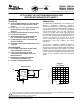

TPS54311, TPS54312
TPS54313, TPS54314
TPS54315, TPS54316
SLVS416B − FEBRUARY 2002 − REVISED APRIL 2005
www.ti.com
4
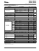
ELECTRICAL CHARACTERISTICS (continued)
T
J
= −40°C to 125°C, VIN = 3 V to 6 V (unless otherwise noted)
PARAMETER TEST CONDITIONS MIN TYP MAX UNIT
ERROR AMPLIFIER
Error amplifier open loop voltage gain
(1)
26 dB
Error amplifier unity gain bandwidth
(1)
3 5 MHz
PWM COMPARATOR
PWM comparator propagation delay time,
PWM comparator input to PH pin (ex-
cluding dead time)
10 mV overdrive
(1)
70 85 ns
SLOW-START/ENABLE
Enable threshold voltage, SS/ENA 0.82 1.20 1.40 V
Enable hysteresis voltage, SS/ENA
(1)
0.03 V
Falling edge deglitch, SS/ENA
(1)
2.5 µs
TPS54311 2.6 3.3 4.1
TPS54312 3.5 4.5 5.4
Internal slow start time
(1)
TPS54313 4.4 5.6 6.7
ms
Internal slow-start time
(1)
TPS54314 2.6 3.3 4.1
ms
TPS54315 3.6 4.7 5.6
TPS54316 4.7 6.1 7.6
Charge current, SS/ENA SS/ENA = 0 V 3 5 8 µA
Discharge current, SS/ENA SS/ENA = 0.2 V, V
I
= 1.5 V 1.5 2.3 4 mA
POWER GOOD
Power good threshold voltage VSENSE falling 90 %V
ref
Power good hysteresis voltage
(1)
3 %V
ref
Power good falling edge deglitch
(1)
35 µs
Output saturation voltage, PWRGD I
(sink)
= 2.5 mA 0.18 0.30 V
Leakage current, PWRGD V
I
= 5.5 V 1 µA
CURRENT LIMIT
Current limit trip point
V
I
= 3 V, output shorted
(1)
4 6.5
A
Current limit trip point
V
I
= 6 V, output shorted
(1)
4.5 7.5
A
Current limit leading edge blanking time
(1)
100 ns
Current limit total response time
(1)
200 ns
THERMAL SHUTDOWN
Thermal shutdown trip point
(1)
135 150 165 °C
Thermal shutdown hysteresis
(1)
10 °C
OUTPUT POWER MOSFETS
r
Power MOSFET switches
V
I
= 6 V
(2)
59 88
mΩ
r
DS(on)
Power MOSFET switches
V
I
= 3 V
(2)
85 136
mΩ
(1)
Specified by design
(2)
Matched MOSFETs, low side r
DS(on)
production tested, high side r
DS(on)
specified by design