
Datasheet

TPS54311, TPS54312
TPS54313, TPS54314
TPS54315, TPS54316
SLVS416B − FEBRUARY 2002 − REVISED APRIL 2005
www.ti.com
6
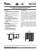
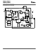
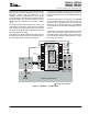
FUNCTIONAL BLOCK DIAGRAM
V
I
Falling
Edge
Deglitch
Enable
Comparator
1.2 V
VIN
2.95 V
Hysteresis: 0.03 V
2.5 µs
Falling
and
Rising
Edge
Deglitch
2.5 µs
VIN UVLO
Comparator
Hysteresis: 0.16 V
Internal/External
Slow-Start
(Internal Slow-Start Time =
3.3 ms to 6.6 ms)
V
I
Feed-Forward
Compensation
−
+
Error
Amplifier
Thermal
Shutdown
145°C
SHUTDOWN
SS_DIS
PWM
Comparator
OSC
Leading
Edge
Blanking
100 ns
RQ
S
Adaptive Dead-Time
and
Control Logic
SHUTDOWN
VIN
REG
VBIAS
VIN
BOOT
VIN
PH
L
OUT
C
O
PGND
PWRGD
Falling
Edge
Deglitch
35 µs
VSENSE
SHUTDOWN
0.90 V
ref
Hysteresis: 0.03 Vref
Power good
Comparator
AGND
VBIAS
ILIM
Comparator
VIN
V
O
FSEL
RTVSENSE
SS/ENA
TPS5431x
5 µA
Reference/
DAC
2 kΩ
40 kΩ
25 ns Adaptive
Deadtime