
Datasheet

TPS54311, TPS54312
TPS54313, TPS54314
TPS54315, TPS54316
SLVS416B − FEBRUARY 2002 − REVISED APRIL 2005
www.ti.com
8
APPLICATION INFORMATION
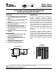
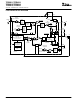
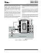
Figure 10 shows the schematic diagram for a typical
TPS54314 application. The TPS54314 (U1) can provide
up to 3 A of output current at a nominal output voltage of
1.8 V. For proper thermal performance, the PowerPAD
underneath the TPS54314 integrated circuit needs to be
soldered to the printed circuit board.
C2
RT
SS/ENA
VBIAS
PWRGD
VSENSE
1
2
3
4
5
6
7
9
VIN
PH
BOOT
PGND
PGND
PGND
PwrPAD
U1
TPS54314PWP
1
2
V
O
GND
J3
C7
0.047 µF
R1
10 kΩ
C11
1000 pF
1
J1
2
1
V
I
GND
+
1
Optional
71.5 kΩ
L1
5.2 µH
R7
8
10 11
12
13
14
15
16
17
18
19
20
AGND
NC
PH
PH
PH
PH
FSEL
VIN
VIN
C8
10 µF
C3
0.1 µF
+
C9
470 µF
4 V
PWRGD
Figure 10. TPS54314 Schematic
INPUT VOLTAGE
The input to the circuit is a nominal 5 VDC, applied at J1.
The optional input filter (C2) is a 220-µF POSCAP
capacitor, with a maximum allowable ripple current of 3 A.
C8 is the decoupling capacitor for the TPS54314 and must
be located as close to the device as possible.
FEEDBACK CIRCUIT
The output voltage of the converter is fed directly into the
VSENSE pin of the TPS54314. The TPS54314 is
internally compensated to provide stability of the output
under varying line and load conditions.
OPERATING FREQUENCY
In the application circuit, a 700 kHz operating frequency is
selected by leaving FSEL open and connecting a 71.5 kΩ
resistor between the RT pin and AGND. Different
operating frequencies may be selected by varying the
value of R3 using equation 1:
R +
500 kHz
Switching Frequency
100 kW
Alternately, preset operating frequencies of 350 kHz or
550 kHz my be selected by leaving RT open and
connecting the FSEL pin to AGND or VIN respectively.
OUTPUT FILTER
The output filter is composed of a 5.2-µH inductor and
470-µF capacitor. The inductor is a low dc resistance
(16-mΩ) type, Sumida CDRH104R−5R2. The capacitor
used is a 4-V POSCAP with a maximum ESR of 40 mΩ.
The output filter components work with the internal
compensation network to provide a stable closed loop
response for the converter.
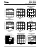
PCB LAYOUT
Figure 11 shows a generalized PCB layout guide for the
TPS54311−16.
The VIN pins should be connected together on the printed
circuit board (PCB) and bypassed with a low ESR ceramic
bypass capacitor. Care should be taken to minimize the
loop area formed by the bypass capacitor connections, the
VIN pins, and the TPS54311−16 ground pins. The
minimum recommended bypass capacitance is 10-µF
ceramic with a X5R or X7R dielectric and the optimum
placement is closest to the VIN pins and the PGND pins.
The TPS54311−16 has two internal grounds (analog and
power). Inside the TPS54311−16, the analog ground ties
to all of the noise sensitive signals, while the power ground
ties to the noisier power signals. Noise injected between
the two grounds can degrade the performance of the
TPS54311−16, particularly at higher output currents.
Ground noise on an analog ground plane can also cause
problems with some of the control and bias signals. For
these reasons, separate analog and power ground traces
are recommended. There should be an area of ground one
the top layer directly under the IC, with an exposed area for
connection to the PowerPAD. Use vias to connect this
ground area to any internal ground planes. Use additional
vias at the ground side of the input and output filter
capacitors as well. The AGND and PGND pins should be
tied to the PCB ground by connecting them to the ground
area under the device as shown. The only components
(1)