
Datasheet

TPS54311, TPS54312
TPS54313, TPS54314
TPS54315, TPS54316
SLVS416B − FEBRUARY 2002 − REVISED APRIL 2005
www.ti.com
9
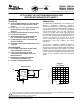
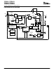
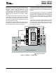
that should tie directly to the power ground plane are the
input capacitors, the output capacitors, the input voltage
decoupling capacitor, and the PGND pins of the
TPS54311−16. Use a separate wide trace for the analog
ground signal path. This analog ground should be used for
the timing resistor RT, slow-start capacitor and bias
capacitor grounds. Connect this trace directly to AGND
(pin 1).
The PH pins should be tied together and routed to the
output inductor. Since the PH connection is the switching
node, inductor should be located very close to the PH pins
and the area of the PCB conductor minimized to prevent
excessive capacitive coupling.
Connect the boot capacitor between the phase node and
the BOOT pin as shown. Keep the boot capacitor close to
the IC and minimize the conductor trace lengths.
Connect the output filter capacitor(s) as shown between
the VOUT trace and PGND. It is important to keep the loop
formed by the PH pins, Lout, Cout and PGND as small as
practical.
Connect the output of the circuit directly to the VSENSE
pin. Do not place this trace too close to the PH trace. Do
to the size of the IC package and the device pinout, they
will have to be routed somewhat close, but maintain as
much separation as possible while still keeping the layout
compact.
Connect the bias capacitor from the VBIAS pin to analog
ground using the isolated analog ground trace. If a
slow-start capacitor or RT resistor is used, or if the SYNC
pin is used to select 350-kHz operating frequency, connect
them to this trace as well.
AGND
BOOT
VSENSE
NC
PWRGD
PH
PH
PH
PH
PH
RT
FSEL
SS/ENA
VBIAS
VIN
VIN
VIN
PGND
PGND
PGND
VOUT
PH
Vin
TOPSIDE GROUND AREA
VIA to Ground Plane
ANALOG GROUND TRACE
EXPOSED
POWERPAD
AREA
OUTPUT INDUCTOR
OUTPUT
FILTER
CAPACITOR
BOOT
CAPACITOR
INPUT
BYPASS
CAPACITOR
INPUT
BULK
FILTER
FREQUENCY SET RESISTOR
SLOW START
CAPACITOR
BIAS CAPACITOR
Figure 11. TPS54311 − 16 PCB Layout