
Datasheet
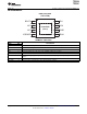

VIN
NC
NC
ENA
GND
VSENSE
BOOT
PH
TPS5430/31
VIN VOUT
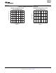
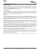
95
60
70
80
90
100
0 0.5 1 1.5 2.5 3 3.5
Efficiency − %
I OutputCurrent A
O
--
EfficiencyvsOutputCurrent
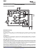
SimplifiedSchematic
V
I
=12V
V =5V
f =500kHz
T =25 C
O
s
A
o
2
50
55
65
75
85
TPS5430
TPS5431
www.ti.com
SLVS632E –JANUARY 2006–REVISED SEPTEMBER 2013
3-A, WIDE INPUT RANGE, STEP-DOWN CONVERTER
Check for Samples: TPS5430 , TPS5431
1
FEATURES
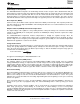
DESCRIPTION
2
• Wide Input Voltage Range:
The TPS5430/TPS5431 is a high-output-current
– TPS5430: 5.5 V to 36 V
PWM converter that integrates a low resistance high
– TPS5431: 5.5 V to 23 V
side N-channel MOSFET. Included on the substrate
with the listed features are a high performance
• Up to 3-A Continuous (4-A Peak) Output
voltage error amplifier that provides tight voltage
Current
regulation accuracy under transient conditions; an
• High Efficiency up to 95% Enabled by 110-mΩ
undervoltage-lockout circuit to prevent start-up until
Integrated MOSFET Switch
the input voltage reaches 5.5 V; an internally set
• Wide Output Voltage Range: Adjustable Down
slow-start circuit to limit inrush currents; and a voltage
to 1.22 V with 1.5% Initial Accuracy
feed-forward circuit to improve the transient
response. Using the ENA pin, shutdown supply
• Internal Compensation Minimizes External
current is reduced to 18 μA typically. Other features
Parts Count
include an active-high enable, overcurrent limiting,
• Fixed 500 kHz Switching Frequency for Small
overvoltage protection and thermal shutdown. To
Filter Size
reduce design complexity and external component
count, the TPS5430/TPS5431 feedback loop is
• Improved Line Regulation and Transient
internally compensated. The TPS5431 is intended to
Response by Input Voltage Feed Forward
operate from power rails up to 23 V. The TPS5430
• System Protected by Overcurrent Limiting,
regulates a wide variety of power sources including
Overvoltage Protection and Thermal Shutdown
24-V bus.
• –40°C to 125°C Operating Junction
The TPS5430/TPS5431 device is available in a
Temperature Range
thermally enhanced, easy to use 8-pin SOIC
• Available in Small Thermally Enhanced 8-Pin
PowerPAD™ package. TI provides evaluation
SOIC PowerPAD™ Package
modules and the Designer software tool to aid in
quickly achieving high-performance power supply
designs to meet aggressive equipment development
APPLICATIONS
cycles.
• Consumer: Set-top Box, DVD, LCD Displays
• Industrial and Car Audio Power Supplies
• Battery Chargers, High Power LED Supply
• 12-V/24-V Distributed Power Systems
1
Please be aware that an important notice concerning availability, standard warranty, and use in critical applications of
Texas Instruments semiconductor products and disclaimers thereto appears at the end of this data sheet.
2PowerPAD is a trademark of Texas Instruments.
PRODUCTION DATA information is current as of publication date.
Copyright © 2006–2013, Texas Instruments Incorporated
Products conform to specifications per the terms of the Texas
Instruments standard warranty. Production processing does not
necessarily include testing of all parameters.