
Datasheet
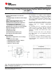
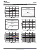

SW
VBST
SS
VFB
GND
8
2
3
4
1
EN
VREG5
7
6
5
VIN
POWER
PAD
TPS54427
DDA
HSOP8
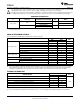
EN
VFB
VREG5
SS
GND
VIN
VIN
VBST
SW
SW
Exposed
Thermal
Die PAD
on
Underside
PGND
1
2
3
4
5
10
9
8
7
6
TPS54427
www.ti.com
SLVSB43A –NOVEMBER 2011–REVISED JUNE 2013
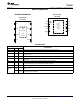
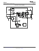
DEVICE INFORMATION
DEVICE INFORMATION
DRC PACKAGE
(TOP VIEW)
DDA PACKAGE
(TOP VIEW)
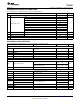
PIN FUNCTIONS
PIN
DESCRIPTION
NAME DDA DRC
EN 1 1 Enable input control. Active high and must be pulled up to enable the device.
VFB 2 2 Converter feedback input. Connect to output voltage with feedback resistor divider.
VREG5 3 3 5.5 V power supply output. A capacitor (typical 1 µF) should be connected to GND. VREG5 is not active
when EN is low.
SS 4 4 Soft-start control. An external capacitor should be connected to GND.
GND 5 5 Ground pin. Power ground return for switching circuit. Connect sensitive SS and VFB returns to GND at a
single point.
SW 6 6, 7 Switch node connection between high-side NFET and low-side NFET.
VBST 7 8 Supply input for the high-side FET gate drive circuit. Connect 0.1µF capacitor between VBST and SW
pins. An internal diode is connected between VREG5 and VBST.
VIN 8 9, 10 Input voltage supply pin.
Exposed Back Thermal pad of the package. Must be soldered to achieve appropriate dissipation. Must be connected to
Thermal side GND.
Pad
Back Thermal pad of the package. PGND power ground return of internal low-side FET. Must be soldered to
side achieve appropriate dissipation.
Copyright © 2011–2013, Texas Instruments Incorporated Submit Documentation Feedback 5
Product Folder Links :TPS54427