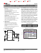
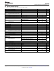
Product Folder Sample & Buy Support & Community Tools & Software Technical Documents TPS54560 SLVSBN0A – MARCH 2013 – REVISED MARCH 2014 TPS54560 4.5 V to 60 V Input, 5 A, Step Down DC-DC Converter with Eco-mode™ 1 Features 3 Description • The TPS54560 is a 60 V, 5 A, step down regulator with an integrated high side MOSFET. The device survives load dump pulses up to 65V per ISO 7637. Current mode control provides simple external compensation and flexible component selection.
TPS54560 SLVSBN0A – MARCH 2013 – REVISED MARCH 2014 www.ti.com Table of Contents 1 2 3 4 5 6 7 8 Features .................................................................. Applications ........................................................... Description ............................................................. Simplified Schematic............................................. Revision History..................................................... Terminal Configuration and Functions................
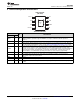
TPS54560 www.ti.com SLVSBN0A – MARCH 2013 – REVISED MARCH 2014 6 Terminal Configuration and Functions HSOIC PACKAGE (TOP VIEW) 8 SW 7 GND 3 6 COMP 4 5 FB BOOT 1 VIN 2 EN RT/CLK Thermal Pad 9 Terminal Functions TERMINAL NAME NO. I/O DESCRIPTION BOOT 1 O A bootstrap capacitor is required between BOOT and SW. If the voltage on this capacitor is below the minimum required to operate the high side MOSFET, the output is switched off until the capacitor is refreshed.
TPS54560 SLVSBN0A – MARCH 2013 – REVISED MARCH 2014 www.ti.com 7 Specifications 7.1 Absolute Maximum Ratings (1) over operating free-air temperature range (unless otherwise noted) MIN MAX VIN –0.3 65 EN –0.3 8.4 BOOT Input voltage 73 –0.3 COMP –0.3 3 RT/CLK –0.3 3.6 –0.
TPS54560 www.ti.com SLVSBN0A – MARCH 2013 – REVISED MARCH 2014 7.5 Electrical Characteristics TJ = –40°C to 150°C, VIN = 4.5 to 60V (unless otherwise noted) PARAMETER TEST CONDITIONS MIN TYP MAX UNIT 60 V 4.3 4.48 V SUPPLY VOLTAGE (VIN TERMINAL) Operating input voltage Internal undervoltage lockout threshold 4.5 Rising 4.1 Internal undervoltage lockout threshold hysteresis 325 mV Shutdown supply current EN = 0 V, 25°C, 4.5 V ≤ VIN ≤ 60 V 2.25 4.
TPS54560 SLVSBN0A – MARCH 2013 – REVISED MARCH 2014 www.ti.com 7.6 Timing Requirements PARAMETER TEST CONDITIONS MIN TYP MAX UNIT –2.2 –3.4 -4.5 μA ENABLE AND UVLO (EN TERMINAL) Hysteresis current Enable to COMP active VIN = 12 V, TA = 25°C 540 µs INTERNAL SOFT-START TIME Soft-Start Time fSW = 500 kHz, 10% to 90% 2.1 ms Soft-Start Time fSW = 2.5 MHz, 10% to 90% 0.
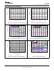
TPS54560 www.ti.com SLVSBN0A – MARCH 2013 – REVISED MARCH 2014 550 500 540 450 FSW - Switching Frequency (kHz) FS - Switching Frequency (kHz) Typical Characteristics (continued) 530 520 510 500 490 480 470 460 450 350 300 250 200 150 100 50 0 ±50 ±25 0 25 50 75 100 125 TJ - Junction Temperature (C) VIN = 12 V 150 200 300 400 500 600 700 800 900 RT/CLK - Resistance (k ) C029 1000 C030 ƒsw (kHz) = 92471 x RT (kΩ)-0.991 RT (kΩ) = 101756 x ƒsw (kHz)-1.
TPS54560 SLVSBN0A – MARCH 2013 – REVISED MARCH 2014 www.ti.com ±3.5 ±0.5 ±3.7 ±0.7 ±3.9 ±0.9 ±4.1 ±1.1 ±4.3 ±1.3 IEN (µA) IEN (uA) Typical Characteristics (continued) ±4.5 ±4.7 ±1.7 ±4.9 ±1.9 ±5.1 ±2.1 ±5.3 ±2.3 ±5.5 ±2.5 ±50 ±25 0 25 50 75 100 125 VIN = 12 V ±50 150 TJ - Junction Temperature (C) ±25 IEN = Threshold +50 mV VIN = 12 V % of Nominal Switching Frequency ±3.1 ±3.3 ±3.5 ±3.7 ±3.9 ±4.1 ±4.3 50 75 100 125 150 C036 IEN = Threshold –50 mV 100 ±2.
TPS54560 www.ti.com SLVSBN0A – MARCH 2013 – REVISED MARCH 2014 210 210 190 190 170 170 IVIN (µA) IVIN (µA) Typical Characteristics (continued) 150 130 150 130 110 110 90 90 70 70 ±50 ±25 0 25 50 75 100 125 TJ - Junction Temperature (C) 150 0 4.5 BOOT-PH UVLO Falling BOOT-PH UVLO Rising 50 60 C042 UVLO Start Switching UVLO Stop Switching 4.4 2.4 4.3 2.3 4.2 VIN (V) VI - BOOT-PH (V) 40 Figure 18. VIN Supply Current vs Input Voltage 2.2 4.1 2.1 4.0 2.0 3.9 1.
TPS54560 SLVSBN0A – MARCH 2013 – REVISED MARCH 2014 www.ti.com 8 Detailed Description 8.1 Overview The TPS54560 is a 60 V, 5 A, step-down (buck) regulator with an integrated high side n-channel MOSFET. The device implements constant frequency, current mode control which reduces output capacitance and simplifies external frequency compensation. The wide switching frequency range of 100 kHz to 2500 kHz allows either efficiency or size optimization when selecting the output filter components.
TPS54560 www.ti.com SLVSBN0A – MARCH 2013 – REVISED MARCH 2014 8.2 Functional Block Diagram EN VIN Thermal Shutdown UVLO Enable Comparator OV Shutdown Shutdown Logic Enable Threshold Boot Charge Voltage Reference Boot UVLO Minimum Clamp Pulse Skip Error Amplifier Current Sense PWM Comparator FB BOOT Logic Shutdown 6 Slope Compensation SW COMP Frequency Foldback Reference DAC for Soft- Start Maximum Clamp Oscillator with PLL 8/8/ 2012 A 0192789 GND POWERPAD RT/ CLK 8.
TPS54560 SLVSBN0A – MARCH 2013 – REVISED MARCH 2014 www.ti.com Feature Description (continued) 8.3.3 Pulse Skip Eco-mode The TPS54560 operates in a pulse skipping Eco-mode at light load currents to improve efficiency by reducing switching and gate drive losses. If the output voltage is within regulation and the peak switch current at the end of any switching cycle is below the pulse skipping current threshold, the device enters Eco-mode.
TPS54560 www.ti.com SLVSBN0A – MARCH 2013 – REVISED MARCH 2014 Feature Description (continued) • • VBOOT = (1.41 x VIN - 0.554 - VF / TSW - 1.847 x 10³ x IB2SW) / (1.41 + 1 / Tsw) RDS(on) = 1 / (-0.3 x VB2SW2 + 3.577 x VB2SW - 4.246) (1) 5.6 5.5 VI - Input Voltage - V 5.4 5.3 5.2 5.1 Dropout Voltage 5 4.9 Dropout Voltage 4.8 4.7 Start 4.6 0 0.05 0.1 0.15 0.2 0.25 0.3 0.35 Stop 0.4 0.45 0.5 Load Current - A Figure 23. 5V Start/Stop Voltage 8.3.
TPS54560 SLVSBN0A – MARCH 2013 – REVISED MARCH 2014 www.ti.com Feature Description (continued) In applications designed to start at relatively low input voltages (that is, from 4.5 V to 9 V) and withstand high input voltages (that is, from 40 V to 60 V), the EN terminal may experience a voltage greater than the absolute maximum voltage of 8.4 V during the high input voltage condition. To avoid exceeding this voltage when using the EN resistors, the EN terminal is clamped internally with a 5.
TPS54560 www.ti.com SLVSBN0A – MARCH 2013 – REVISED MARCH 2014 Feature Description (continued) 8.3.10 Accurate Current Limit Operation and Maximum Switching Frequency The TPS54560 implements peak current mode control in which the COMP terminal voltage controls the peak current of the high side MOSFET. A signal proportional to the high side switch current and the COMP terminal voltage are compared each cycle.
TPS54560 SLVSBN0A – MARCH 2013 – REVISED MARCH 2014 www.ti.
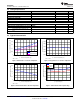
TPS54560 www.ti.com SLVSBN0A – MARCH 2013 – REVISED MARCH 2014 Feature Description (continued) TPS54560 TPS54560 RT/CLK RT/CLK PLL PLL RT Hi-Z Clock Source Clock Source RT Figure 27. Synchronizing to a System Clock SW SW EXT EXT IL IL Figure 28. Plot of Synchronizing in CCM Figure 29. Plot of Synchronizing in DCM SW EXT IL Figure 30.
TPS54560 SLVSBN0A – MARCH 2013 – REVISED MARCH 2014 www.ti.com Feature Description (continued) 8.3.12 Overvoltage Protection The TPS54560 incorporates an output overvoltage protection (OVP) circuit to minimize voltage overshoot when recovering from output fault conditions or strong unload transients in designs with low output capacitance. For example, when the power supply output is overloaded the error amplifier compares the actual output voltage to the internal reference voltage.
TPS54560 www.ti.com SLVSBN0A – MARCH 2013 – REVISED MARCH 2014 Feature Description (continued) 8.3.15 Simple Small Signal Model for Peak Current Mode Control Figure 32 describes a simple small signal model that can be used to design the frequency compensation. The TPS54560 power stage can be approximated by a voltage-controlled current source (duty cycle modulator) supplying current to the output capacitor and load resistor.
TPS54560 SLVSBN0A – MARCH 2013 – REVISED MARCH 2014 www.ti.com Feature Description (continued) æ s ç1 + 2p ´ fZ VOUT = Adc ´ è VC æ s ç1 + 2p ´ fP è Adc = gmps ´ RL ö ÷ ø ö ÷ ø (10) (11) 1 fP = COUT ´ RL ´ 2p (12) 1 fZ = COUT ´ RESR ´ 2p (13) 8.3.16 Small Signal Model for Frequency Compensation The TPS54560 uses a transconductance amplifier for the error amplifier and supports three of the commonlyused frequency compensation circuits.
TPS54560 www.ti.com SLVSBN0A – MARCH 2013 – REVISED MARCH 2014 Feature Description (continued) Aol A0 P1 Z1 P2 A1 BW Figure 34.
TPS54560 SLVSBN0A – MARCH 2013 – REVISED MARCH 2014 www.ti.com 8.4 Device Functional Modes 8.4.1 Operation with VIN < 4.5 V (Minimum VIN) The device is recommended to operate with input voltages above 4.5 V. The typical VIN UVLO threshold is 4.3 V and the device may operate at input voltages down to the UVLO voltage. At input voltages below the actual UVLO voltage, the device will not switch.
TPS54560 www.ti.com SLVSBN0A – MARCH 2013 – REVISED MARCH 2014 Device Functional Modes (continued) 8.4.3.2 Split Rail Power Supply The TPS54560 can be used to convert a positive input voltage to a split rail positive and negative output voltage by using a coupled inductor. Idea applications are amplifiers requiring a split rail positive and negative voltage power supply. For a more detailed example see SLVA369.
TPS54560 SLVSBN0A – MARCH 2013 – REVISED MARCH 2014 www.ti.com 9 Application and Implementation 9.1 Application Information The TPS54560 is a 60 V, 5 A, step down regulator with an integrated high side MOSFET. Idea applications are: 12 V, 24 V and 48 V Industrial, automotive and communications power systems 9.2 Typical Application L1 7.2uH 5V, 5A VOUT C4 0.1uF U1 TPS54560DDA 7V to 60V 2 3 C10 C3 2.2uF C1 2.2uF C2 2.2uF 2.
TPS54560 www.ti.com SLVSBN0A – MARCH 2013 – REVISED MARCH 2014 The typical minimum on time, tonmin, is 135 ns for the TPS54560. For this example, the output voltage is 5 V and the maximum input voltage is 60 V, which allows for a maximum switch frequency up to 708 kHz to avoid pulse skipping from Equation 8. To ensure overcurrent runaway is not a concern during short circuits use Equation 9 to determine the maximum switching frequency for frequency foldback protection.
TPS54560 SLVSBN0A – MARCH 2013 – REVISED MARCH 2014 LO(min ) = VIN(max ) - VOUT IOUT ´ KIND ´ www.ti.com VOUT 60 V - 5 V 5V = ´ = 7.6 mH VIN(max ) ´ fSW 5 A x 0.3 60 V ´ 400 kHz (27) spacer IRIPPLE = VOUT ´ (VIN(max ) - VOUT ) VIN(max ) ´ LO ´ fSW = 5 V x (60 V - 5 V) = 1.591 A 60 V x 7.2 mH x 400 kHz (28) spacer ( æ 1 ç VOUT ´ VIN(max ) - VOUT 2 IL(rms ) = (IOUT ) + ´ 12 çç VIN(max ) ´ LO ´ fSW è )÷ö 2 ÷ = ÷ ø 2 (5 A ) 2 æ 5 V ´ (60 V - 5 V ) ö 1 + ´ ç ÷ =5A ç ÷ 12 è 60 V ´ 7.
TPS54560 www.ti.com SLVSBN0A – MARCH 2013 – REVISED MARCH 2014 Capacitance de-ratings for aging, temperature and dc bias increases this minimum value. For this example, 3 x 47 μF, 10 V ceramic capacitors with 5 mΩ of ESR will be used. The derated capacitance is 87.4 µF, well above the minimum required capacitance of 62.5 µF. Capacitors are generally rated for a maximum ripple current that can be filtered without degrading capacitor reliability.
TPS54560 SLVSBN0A – MARCH 2013 – REVISED MARCH 2014 www.ti.com 9.2.2.5 Input Capacitor The TPS54560 requires a high quality ceramic type X5R or X7R input decoupling capacitor with at least 3 μF of effective capacitance. Some applications will benefit from additional bulk capacitance. The effective capacitance includes any loss of capacitance due to dc bias effects. The voltage rating of the input capacitor must be greater than the maximum input voltage.
TPS54560 www.ti.com SLVSBN0A – MARCH 2013 – REVISED MARCH 2014 9.2.2.7 Undervoltage Lockout Set Point The Undervoltage Lockout (UVLO) can be adjusted using an external voltage divider on the EN terminal of the TPS54560. The UVLO has two thresholds, one for power up when the input voltage is rising and one for power down or brown outs when the input voltage is falling. For the example design, the supply should turn on and start switching once the input voltage increases above 6.5 V (UVLO start).
TPS54560 SLVSBN0A – MARCH 2013 – REVISED MARCH 2014 www.ti.com To determine the compensation resistor, R4, use Equation 46. Assume the power stage transconductance, gmps, is 17 A/V. The output voltage, VO, reference voltage, VREF, and amplifier transconductance, gmea, are 5 V, 0.8 V and 350 μA/V, respectively. R4 is calculated to be 16.8 kΩ and a standard value of 16.9 kΩ is selected. Use Equation 47 to set the compensation zero to the modulator pole frequency.
TPS54560 www.ti.com SLVSBN0A – MARCH 2013 – REVISED MARCH 2014 PTOT = PCOND + PSW + PGD + PQ = 0.958 W + 0.118 W + 0.014 W + 0.0018 W = 1.092 W For given TA, TJ = TA + RTH ´ PTOT (54) (55) For given TJMAX = 150°C TA (max ) = TJ(max ) - RTH ´ PTOT where • • • • • • Ptot is the total device power dissipation (W) TA is the ambient temperature (°C). TJ is the junction temperature (°C).
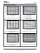
TPS54560 SLVSBN0A – MARCH 2013 – REVISED MARCH 2014 www.ti.com 1 A/div 10 V/div 9.2.3 Application Curves VIN 10 mV/div 200 mV/div IOUT VOUT ±5V offset VOUT ±5V offset Time = 4 ms/div Time = 100 Ps/div Figure 39. Line Transient (8 V to 40 V) 2 V/div EN 4 V/div 4 V/div VIN VIN 1 V/div 5 V/div 5 V/div Figure 38. Load Transient VOUT EN VOUT Time = 2 ms/div Time = 2 ms/div Figure 41. Start-up With EN Figure 40.
TPS54560 www.ti.com SLVSBN0A – MARCH 2013 – REVISED MARCH 2014 10 V/div 1 m\A/div IL 200 mV/div 10 V/div IL 10 mV/div 200 mA/div SW SW VOUT ± AC Coupled VIN ± AC Coupled Time = 1 ms/div Time = 4 Ps/div No Load Figure 44. Output Ripple PSM Figure 45. Input Ripple CCM IL 200 mA/div SW 20 mV/div 10 mV/div 500 mA/div 10 V/div 2 V/div SW VIN ± AC Coupled IL VOUT Time = 4 Ps/div Time = 40 Ps/div IOUT = 100 mA No Load Figure 47. Low Dropout Operation 2 V/div 2 V/div Figure 46.
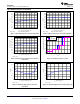
TPS54560 SLVSBN0A – MARCH 2013 – REVISED MARCH 2014 www.ti.com 100 100 90 95 80 70 Efficiency (%) Efficiency (%) 90 85 80 75 60 50 40 30 70 20 VIN =Series4 7V VIN =36V 36 V 65 60 0 0.5 1 1.5 2 VIN =12V 12 V VIN =24V 24 V VIN =48V 48 V VIN =60V 60 V 2.5 3 3.5 4 4.5 0 0.001 0.00 5 IO - Output Current (A) VOUT = 5 V VOUT = 5 V ƒsw = 400 kHz VIN = 60 60VV 0.10 1.00 C024 ƒsw = 400 kHz Figure 51.
TPS54560 www.ti.com SLVSBN0A – MARCH 2013 – REVISED MARCH 2014 0.6 0.3 Output Voltage Normalized (%) Output Voltage Normalized (%) 0.5 0.4 0.3 0.2 0.1 ±0.0 ±0.1 ±0.2 ±0.3 ±0.4 0.2 0.1 0.0 ±0.1 ±0.2 ±0.5 ±0.6 0.0 0.5 1.0 1.5 2.0 2.5 3.0 3.5 4.0 IO - Output Current (A) VIN = 12 V VOUT = 5 V 4.5 5.0 ±0.3 5 10 15 ƒsw = 400 kHz 20 25 30 35 40 45 50 55 VI - Input Voltage (V) C024 VOUT = 5 V Figure 56. Regulation vs Load Current IOUT = 5 A 60 C024 ƒsw = 400 kHz Figure 57.
TPS54560 SLVSBN0A – MARCH 2013 – REVISED MARCH 2014 www.ti.com 11 Layout 11.1 Safe Operating Area 90 90 80 80 70 70 60 60 TA (C) TA (C) The safe operating area (SOA) of the device is shown in Figure 58, through Figure 61 for 3.3 V, 5 V and 12 V outputs and varying amounts of forced air flow. The temperature derating curves represent the conditions at which the internal and external components are at or below the manufacturer’s maximum operating temperatures.
TPS54560 www.ti.com SLVSBN0A – MARCH 2013 – REVISED MARCH 2014 11.2 Layout Guidelines Layout is a critical portion of good power supply design. There are several signal paths that conduct fast changing currents or voltages that can interact with stray inductance or parasitic capacitance to generate noise or degrade performance. • To reduce parasitic effects, the VIN terminal should be bypassed to ground with a low ESR ceramic bypass capacitor with X5R or X7R dielectric.
TPS54560 SLVSBN0A – MARCH 2013 – REVISED MARCH 2014 www.ti.com 12 Device and Documentation Support 12.1 Trademarks Eco-mode, PowerPAD, WEBENCH are trademarks of Texas Instruments. 12.2 Electrostatic Discharge Caution These devices have limited built-in ESD protection. The leads should be shorted together or the device placed in conductive foam during storage or handling to prevent electrostatic damage to the MOS gates. 12.3 Glossary SLYZ022 — TI Glossary.
PACKAGE OPTION ADDENDUM www.ti.
PACKAGE OPTION ADDENDUM www.ti.com 31-Oct-2013 In no event shall TI's liability arising out of such information exceed the total purchase price of the TI part(s) at issue in this document sold by TI to Customer on an annual basis.
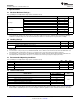
PACKAGE MATERIALS INFORMATION www.ti.com 6-Sep-2013 TAPE AND REEL INFORMATION *All dimensions are nominal Device TPS54560DDAR Package Package Pins Type Drawing SO Power PAD DDA 8 SPQ Reel Reel A0 Diameter Width (mm) (mm) W1 (mm) 2500 330.0 12.8 Pack Materials-Page 1 6.4 B0 (mm) K0 (mm) P1 (mm) 5.2 2.1 8.0 W Pin1 (mm) Quadrant 12.
PACKAGE MATERIALS INFORMATION www.ti.com 6-Sep-2013 *All dimensions are nominal Device Package Type Package Drawing Pins SPQ Length (mm) Width (mm) Height (mm) TPS54560DDAR SO PowerPAD DDA 8 2500 366.0 364.0 50.
IMPORTANT NOTICE Texas Instruments Incorporated and its subsidiaries (TI) reserve the right to make corrections, enhancements, improvements and other changes to its semiconductor products and services per JESD46, latest issue, and to discontinue any product or service per JESD48, latest issue. Buyers should obtain the latest relevant information before placing orders and should verify that such information is current and complete.