User's Guide SLUU896 – March 2012 Using the TPS59650EVM-753 Intel™ IMVP-7 3-Phase CPU/2-Phase GPU SVID Power System The TPS59650EVM-753 evaluation module (EVM) is a complete solution for Intel™ IMVP7 Serial VID(SVID) Power System from a 9V-20V input bus. This EVM uses the TPS59650 for IMVP7 - 3-Phase CPU and 2-Phase GPU Vcore controller, the TPS51219 for 1.05VCCIO, TPS51916 for DDR3L/DDR4 Memory rail (1.2VDDQ, 0.6VTT and 0.
www.ti.com 3 USB Cable ................................................................................................................... 8 4 TPS59650EVM-753 Recommended Test Set Up ..................................................................... 10 5 TPS59650EVM-753 CPU GUI set up Window ........................................................................ 15 6 TPS59650EVM-753 GPU GUI set up Window ........................................................................
www.ti.com 52 53 54 55 56 57 58 59 60 61 62 63 64 65 66 67 68 69 70 71 72 73 74 75 76 77 78 79 80 81 82 83 84 85 86 87 88 89 90 91 92 93 94 95 96 97 98 99 ................................................................................ GPU2 Dynamic VID:SetVID-Fast/Fast ................................................................................. GPU2 Dynamic VID:SetVID-Decay/Fast ...............................................................................
www.ti.com 100 TPS59650EVM-753 Internal Layer 6 ................................................................................... 46 101 TPS59650EVM-753 Internal Layer 7 ................................................................................... 46 List of Tables 1 TPS59650EVM-753 Electrical Performance Specifications ........................................................... 7 2 Current Limit Trip Selection .................................................................................
Description www.ti.com 1 Description The TPS59650EVM-753 is designed to use a 9V-20V Input bus to produce 6 regulated outputs for IMVP7 SVID CPU/GPU Power System. The TPS59650EVM-753 is specially designed to demonstrate the TPS59650 full IMVP7 mobile feature while providing GUI communication programing and a number of test points to evaluate the static and dynamic performance of TPS59650. 1.1 Typical Applications • 1.
TPS59650EVM-753 Power System Block Diagram 2 www.ti.com TPS59650EVM-753 Power System Block Diagram IMVP7 TPS59650 9-20VBAT Power Block CPU Core (94A) 48 Pin 6x6 QFN SVID GPU Core (46A) TPS51219 16 Pin 3x3 QFN TPS51916 20 Pin 3x3 QFN TPS70102PWP 5Vin 20 Pin PWP VCCIO: 1.05V/10A DDR3L/DDR4 Memory Rail VDDQ: 1.2V/8A VTT: 0.6V/2A, VTTREF: 0.6V/10mA 1.8V/500mA 3.
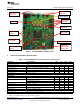
Electrical Performance Specifications www.ti.com CPU/GPU VR_ON CPU Load Connector CSD87350Q5D OCL, FSW selection CPU Core TPS59650 TPS51219 VCCIO GPU CORE Intel SVID GUI from USB GPU Load Connector TPS51916 DDR3L/DDR4 Memory Rail Chief River CPU socket Figure 2. TPS59650EVM-753 EVM Illustration 3 Electrical Performance Specifications Table 1.
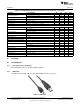
Test Setup www.ti.com Table 1. TPS59650EVM-753 Electrical Performance Specifications (1) (continued) PARAMETER Output voltage regulation Output voltage ripple TEST CONDITIONS MIN TYP MAX UNITS Line regulation 0.1% Load regulation(Droop) Load Line –3.9 mΩ 30 mVpp VBAT=12V, 1.23V/50A 2 Phase at 385kHz Output load current 0 Output over current Selectable per phase Switching frequency Selectable Full load efficiency VBAT=12V, 1.
Test Setup www.ti.com 4.1.3 1. 2. 3. 4. 4.1.4 TPS59650 USB driver and SVID GUI Installation Copy the both files: setup.exe and setup.msi to the host computer. Run this setup.exe. Following installation Instructions, this will install the driver and the Texas Instruments SVID GUI. It will add the below icon DC Source 12VBAT DC Source: The 12VBAT DC source should be a 0-20V variable DC source capable of supplying 20Adc current. Connect 12VBAT to J21 as shown in Figure 4.
Test Setup www.ti.com 12VBAT DC Source - - - + V3 VCCIO + CPU - + + Load - + - + 5Vin DC Source + - V2 A1 - + V1 - + + - GPU + USB Cable A B Host Computer + _ VDDQ Figure 4. TPS59650EVM-753 Recommended Test Set Up 4.4 USB Cable Connections A standard USB_A and 5 pin Mini_B USB cable needed to connect between host computer and J34 USB port (left bottom side). A GREEN LED(D13) will light up near the USB port on the EVM. This just means USB cable is connected. 4.
Configuration www.ti.com 4.6 Output Connections 1. Connect Load to J1, J2, J3 and set Load to constant resistance mode to sink 0Adc before 5Vin and 12VBAT are applied. This is for CPU operation. 2. Connect a voltmeter V3 at J7 to measure CPU Vcore sense voltage. 5 Configuration All Jumper selections should be made prior to applying power to the EVM. User can configure this EVM per following configurations. 5.1 5.1.
Configuration 5.1.3 www.ti.com GPU Frequency Selection (J13) The operating frequency can be set by J13 Default setting: 385 kHz for GPU. Table 4. GPU Frequency Selection Jumper set to Connected Resistor GPU Left (1-2 pin shorted) 150k 660 kHz 2nd(3-4 pin shorted) 100k 605 kHz 3 (5-6 pin shorted) 75k 550 kHz 4th(7-8 pin shorted) 56.2k 495 kHz 5th(9-10 pin shorted) 39.2k 440 kHz 6th(11-12 pin shorted) 30.1k 385 kHz 7th(13-14 pin shorted) 24.3k 330 kHz Right(15-16 pin shorted) 20.
Configuration www.ti.com 5.1.7 IMVP-7 VR_ON Enable Selection (S4) The IMVP-7 CPU/GPU can be enabled and disabled by S4 Default setting: Push S4 to “OFF” position to disable both CPU and GPU Table 8. VR_ON Enable Selection 5.2 5.2.1 Switch set to VR_ON Selection Push S4 to “ON” position Enable IMVP-7 CPU/GPU Vcore Push S4 to “OFF” position Disable IMVP-7 CPU/GPU Vcore 1.2VDDQ, 0.6V VTT and 0.
Test Procedure 5.3.3 www.ti.com On Board Dyanamic Load Enable Pin (J23) The on board dynamic load can be enabled or disabled by J23 Default setting: Jumper shorts on J23 Table 12. On Board Dynamic Load Enable/Disable selection Jumper set to Selection Jumper shorts Enable on board dynamic load No Jumper short Disable on board dynamic load 6 Test Procedure 6.1 Line/Load Regulation and Efficiency Measurement Procedure 6.1.1 1. 2. 3. 4. 5. 6. 7. 8. 9. CPU Set up EVM as described in Section 4.
Test Procedure www.ti.com Figure 5. TPS59650EVM-753 CPU GUI set up Window 6.1.2 1. 2. 3. 4. 5. GPU Connect the LOAD to GPU terminal J4, J5 and V3 at J9. Ensure correct polarity. Add scope probe on the TP46 for GPU Vcore_G ripple measurement Push S4 to “ON” position to enable the VR_ON of TPS59650. The VR_ON LED will light up. Now you are ready to send SVID commends for GPU. Using pull-down menu: Address: 01 GPU, Commend: SetVIDslow, Payload: 1.
Test Procedure www.ti.com Figure 6. TPS59650EVM-753 GPU GUI set up Window 6. Measure V3: GPU Vcore_G at J9 and A1: 12VBAT input current 7. Vary GPU LOAD from 0Adc to 50Adc, GPU Vcore must remain in load line 8. Vary 12VBAT from 9V to 20V GPU Vcore must remain in line regulation 9. Push S4 to “OFF” position to disable GPU Vcore controller. 10. Decrease LOAD to 0A and disconnect the LOAD from terminal J11 11. Disconnect V3 from J9. 12. Disconnect scope probe from TP46 13.
Test Procedure www.ti.com 6.1.3 VDDQ 1. Connect the LOAD to VDDQ terminal J19 and V3 at J20. Ensure correct polarity. 2. Remove Jumper from J17, J18 from pin2 and pin3 and put this Jumper on pin1 and pin 2 of J18, J17 to enable S5 of VDDQ controller. VDDQ PGOOD LED will light up. 3. Measure V3: VDDQ at J20 and A1: 12Vin input current 4. Vary VDDQ LOAD from 0Adc to 8Adc, VDDQ must remain in the load regulation 5. Vary 12VBAT from 9V to 20V, VDDQ must remain in the line regulation 6.
Performance Data and Typical Characteristic Curves 7 www.ti.com Performance Data and Typical Characteristic Curves Figure 7 through Figure 91 present typical performance curves for TPS59650EVM-753. Jumpers set to default locations, see section 6 of this user’s guide. 7.1 CPU 3-Phase Operation 95 1.1 VIN = 12 V VIN = 9 V 85 Efficiency - % VIN = 9 V 1.05 VO - Output Voltage - V 90 VIN = 20 V 80 75 SPEC(max) 1 VIN = 12 V 0.95 VIN = 20 V 0.9 SPEC(min) SPEC(nom) 0.
Performance Data and Typical Characteristic Curves www.ti.com TPS59650EVM CPU Switching node and Output Ripple Test condition: 12 Vin, 1.05V/60A CPU 3 Phase operation TPS59650EVM CPU Dynamic VID: Set VID-Slow/Slow Test condition: 12 Vin, 1.05V/1A CPU 3 Operation CH1: CSW1 CH1: CSW1 CH2: CSW2 CH2: CSW2 CH3: 1.05V core CH3: CSW3 CH4: VDIO CH4: 1.05V core Ripple Figure 11. CPU3 Switching Node(Ripple) Figure 12. CPU3 Dynamic VID: SetVID-Slow/Slow TPS59650EVM Test condition: 12 Vin, 1.
Performance Data and Typical Characteristic Curves www.ti.com Test condition: 12 Vin, 1.05V/0A-51A CPU 3 Phase on board dynamic load TPS59650EVM CPU Output Load Releas with OSR/USR middle level Test condition: 12 Vin, 1.05V/0A-51A CPU 3 Phase on board dynamic load TPS59650EVM CPU Output Load Insertion with OSR/USR middle level CH1: CSW1 CH1: CSW1 CH2: CSW2 CH2: CSW2 CH3: CSW3 CH3: CSW3 CH4: 1.05V core CH4: 1.05V core Figure 15. CPU3 Output Load Insertion with OSR/USR middle level Figure 16.
Performance Data and Typical Characteristic Curves www.ti.com Figure 18. CPU3 MOSFET 7.2 Figure 19. CPU3 IC CPU 2-Phase Operation 1.1 95 VIN = 12 V VIN = 12 V VIN = 9 V 90 VO - Output Voltage - V 1.05 Efficiency - % 85 VIN = 20 V 80 75 VIN = 9 V 1 SPEC(min) SPEC(nom) 0.95 SPEC(max) 0.9 70 65 0 VIN = 20 V 5 10 15 20 25 30 35 40 IO - Output Current - A Figure 20. CPU2 Efficiency SLUU896 – March 2012 Submit Documentation Feedback 45 50 55 0.
Performance Data and Typical Characteristic Curves www.ti.com TPS59650EVM Test condition: 12 Vin, 1.05V/40A TPS59650EVM Test condition: 12 Vin, 1.05V/40A CPU VDIO Turn on CPU 2 Phase Operation CPU VR_ON Turn off CPU 2 Phase Operation CH1: CSW1 CH1: CSW1 CH2: CSW2 CH2: CSW2 CH3: 1.05V core CH3: 1.05V core CH4: CPGOOD CH4: CPGOOD Figure 22. CPU2 Enable Turn on Figure 23. CPU2 Enable Turn off TPS59650EVM Test condition: 12 Vin, 1.
Performance Data and Typical Characteristic Curves www.ti.com TPS59650EVM Test condition: 12 Vin, 1.05V/1A TPS59650EVM Test condition: 12 Vin, 1.05V/1A CPU Dynamic VID: Set VID-Slow/Slow CPU 2 Operation CPU Dynamic VID: Set VID-Decay/Fast CPU 2 Operation CH1: CSW1 CH1: CSW1 CH2: CSW2 CH2: CSW2 CH3: 1.05Vcore CH3: 1.05Vcore CH4: VDIO CH4: VDIO Figure 26. CPU2 Dynamic VID:SetVID-Fast/Fast TPS59650EVM CPU Output Load Insertion with OSR/USR middle level Test condition: 12 Vin, 1.
Performance Data and Typical Characteristic Curves www.ti.com Figure 30. CPU2 Bode Plot at 12Vin, 1.05V/55A Test condition: CPU2 12Vin, 1.05V/55A no airflow Figure 31. CPU2 MOSFET 24 Using the TPS59650EVM-753 Intel™ IMVP-7 3-Phase CPU/2-Phase GPU SVID Power System Copyright © 2012, Texas Instruments Incorporated Figure 32.
Performance Data and Typical Characteristic Curves www.ti.com 7.3 CPU1-Phase Operation 1.1 95 VIN = 12 V VIN = 12 V VIN = 20 V VIN = 9 V 90 VO - Output Voltage - V Efficiency - % 1.05 85 VIN = 20 V 80 VIN = 9 V 1 SPEC(min) SPEC(nom) SPEC(max) 0.95 75 70 0 5 10 15 20 25 IO - Output Current - A 30 Figure 33. CPU1 Efficiency TPS59650EVM CPU VDIO Turn on 35 0.9 0 5 10 15 20 25 IO - Output Current - A 30 35 Figure 34. CPU1 Load regulation Test condition: 12 Vin, 1.
Performance Data and Typical Characteristic Curves TPS59650EVM CPU Switching Node Test condition: 12 Vin, 1.05V/20A CPU 1 Phase operation www.ti.com TPS59650EVM CPU Switching Node and Output Ripple Test condition: 12 Vin, 1.05V/20A CPU 1 Phase operation CH1: CSW1 CH1: CSW1 CH2: 1.05Vcore Ripple Figure 37. CPU1 Switching Node TPS59650EVM CPU Dynamic VID: Set VID-Slow/Slow Figure 38. CPU1 Switching node and Ripple Test condition: 12 Vin, 1.
Performance Data and Typical Characteristic Curves www.ti.com TPS59650EVM CPU Dynamic VID: Set VID-Decay/Fast Test condition: 12 Vin, 1.05V/1A CPU 1 Operation TPS59650EVM CPU Output Load Insertion with OSR/USR middle level Test condition: 12 Vin, 1.05V/0A-27A CPU 1 Phase on board dynamic load CH1: CSW1 CH1: DYN_C CH2: CSW1 CH3: 1.05Vcore CH4: VDIO CH3: 1.05Vcore Figure 41. CPU1 Dynamic VID:SetVID-Decay/Fast TPS59650EVM CPU Output Load Releas with OSR/USR middle level Figure 42.
Performance Data and Typical Characteristic Curves www.ti.com Figure 44. CPU1 Bode Plot at 12Vin, 1.05V/33A Test condition: CPU1 12Vin, 1.05V/33A no airflow Figure 45. CPU1 MOSFET 28 Using the TPS59650EVM-753 Intel™ IMVP-7 3-Phase CPU/2-Phase GPU SVID Power System Copyright © 2012, Texas Instruments Incorporated Figure 46.
Performance Data and Typical Characteristic Curves www.ti.com 7.4 GPU 2 Phase Operation 95 1.3 VIN = 12 V VIN = 9 V VO - Output Voltage - V VIN = 20 V Efficiency - % VIN = 9 V 1.25 90 85 VIN = 20 V 1.2 1.15 80 75 70 0 VIN = 12 V SPEC(min) 1.1 SPEC(nom) 1.05 5 10 15 20 25 30 35 IO - Output Current - A 40 45 Figure 47. GPU2 Efficiency TPS59650EVM GPU VDIO Turn on 50 SPEC(max) 1 0 5 10 15 20 25 30 35 IO - Output Current - A 45 50 Figure 48.
Performance Data and Typical Characteristic Curves TPS59650EVM GPU Switching Node and Output Ripple www.ti.com Test condition: 12 Vin, 1.23V/20A GPU 2 Phase operation TPS59650EVM Test condition: 12 Vin, 1.23V/1A GPU Dynamic VID: Set VID-Slow/Slow GPU 2 Operation CH1: GSW1 CH2: GSW1 CH2: GSW2 CH3: GSW2 CH3: 1.23Vcore_G CH4: VDIO CH4: 1.23Vcore Ripple Figure 51. GPU2 Switching Node and Ripple Figure 52. GPU2 Dynamic VID:SetVID-Slow/Slow TPS59650EVM Test condition: 12 Vin, 1.
Performance Data and Typical Characteristic Curves www.ti.com Test condition: 12 Vin, 1.23V/0A-18A TPS59650EVM GPU Output Load Insertion with OSR/USR GPU 2 Phase on board dynamic load least reduction TPS59650EVM GPU Output Load Release with OSR/USR least reduction CH1: DYN_G Test condition: 12 Vin, 1.23V/0A-18A GPU 2 Phase on board dynamic load CH1: DYN_G CH2: GSW1 CH2: GSW1 CH3: GSW2 CH3: GSW2 CH4: 1.23Vcore CH4: 1.23Vcore Figure 55. GPU2 Output Load Insertion with OSR/USR Figure 56.
Performance Data and Typical Characteristic Curves www.ti.com Figure 58. GPU2 MOSFET 7.5 Figure 59. GPU2 IC GPU 1 Phase Operation 95 1.3 VIN = 9 V 90 1.25 VO - Output Voltage - V Efficiency - % VIN = 12 V 85 VIN = 20 V 80 1.2 VIN = 12 V SPEC(min) VIN = 20 V VIN = 9 V 1.1 5 10 15 20 25 IO - Output Current - A 30 35 1.05 0 Figure 60. GPU1 Efficiency 32 SPEC(nom) 1.15 75 70 0 SPEC(max) 5 10 15 20 25 IO - Output Current - A 30 35 Figure 61.
Performance Data and Typical Characteristic Curves www.ti.com TPS59650EVM GPU VDIO Turn on Test condition: 12 Vin, 1.05V/20A GPU 1 Phase operation TPS59650EVM GPU VR_ON Turn on Test condition: 12 Vin, 1.23V/20A GPU 1 Phase operation CH1: VR_ON CH1: VDIO CH2: GSW1 CH2: GSW1 CH3: 1.23Vcore CH3: 1.23Vcore CH4: GPGOOD CH4: GPGOOD Figure 62. GPU1 Enable Turn on TPS59650EVM GPU Switching Node Test condition: 12 Vin, 1.23V/0A-18A GPU 1 Phase operation Figure 63.
Performance Data and Typical Characteristic Curves www.ti.com TPS59650EVM Test condition: 12 Vin, 1.23V/1A TPS59650EVM Test condition: 12 Vin, 1.23V/1A GPU Dynamic VID: Set VID-Slow/Slow GPU 1 Operation CPU Dynamic VID: Set VID-Fast/Fast GPU 1 Operation CH1: GSW1 CH1: CSW1 CH3: 1.23Vcore_G CH3: 1.23Vcore_G CH4: VDIO CH4: VDIO Figure 66. GPU1 Dynamic VID:SetVID-Slow/Slow TPS59650EVM Test condition: 12 Vin, 1.23V/1A GPU Dynamic VID: Set VID-Decay/Fast GPU 1 Operation Figure 67.
Performance Data and Typical Characteristic Curves www.ti.com Test condition: 12 Vin, 1.23V/0A-18A TPS59650EVM GPU Output Load Release with OSR/USR GPU 1 Phase on board dynamic load least reduction CH1: DYN_G CH2: GSW1 CH3: 1.23Vcore Figure 70. GPU1 Output Load Release with OSR/USR OFF Figure 71. GPU1 Bode Plot at 12Vin, 1.23V/33A Test condition: GPU1 12Vin, 1.
Performance Data and Typical Characteristic Curves www.ti.com Figure 72. GPU1 MOSFET 7.6 Figure 73. GPU1 IC 1.05V VCCIO 100 1.08 VIN = 9 V 90 80 Efficiency - % 60 VO - Output Voltage - V VIN = 12 V 70 VIN = 20 V 50 40 30 1.06 VIN = 12 V VIN = 9 V VIN = 20 V 1.04 20 10 0 0.001 0.01 0.1 1 IO - Output Current - A 10 100 1.02 Figure 74. 1.05V Efficiency 36 0 2 4 6 IO - Output Current - A 8 10 Figure 75. 1.
Performance Data and Typical Characteristic Curves www.ti.com TPS59650EVM VCCIO Enable Turn on Test condition: 12 Vin, 1.05VCCIO/10A Test condition: 12 Vin, 1.05VCCIO/10A CH1: VCCIO_EN CH1: VCCIO_EN CH2: 1.05VCCIO CH2: 1.05VCCIO CH3: VCCIO_PG CH3: VCCIO_PG Figure 76. 1.05V Enable Turn on TPS59650EVM VCCIO Switching Node TPS59650EVM VCCIO Enable Turn off Test condition: 12 Vin, 1.05VCCIO/10A Figure 77. 1.05V Enable Turn off TPS59650EVM VCCIO Output Ripple Test condition: 12 Vin, 1.
Performance Data and Typical Characteristic Curves TPS59650EVM VCCIO Output Transient from DCM to CCM Test condition: 12 Vin, 1.05VCCIO/0A-10A www.ti.com TPS59650EVM VCCIO Output Transient from CCM to DCM CH1: VCCIO Output Test condition: 12 Vin, 1.05VCCIO/0A-10A CH1: VCCIO Output CH2: VCCIO Output current CH2: VCCIO Output current Figure 80. 1.05V Transient DCM TO CCM Figure 81. 1.05V Transient CCM to DCM Test condition: 12Vin, 1.05V/10A no airflow Figure 82.
Performance Data and Typical Characteristic Curves www.ti.com 7.7 1.2V VDDQ 1.26 100 90 VIN = 9 V 1.24 80 VIN = 12 V VO - Output Voltage - V Efficiency - % 70 VIN = 20 V 60 50 40 30 1.22 VIN = 12 V VIN = 20 V 1.20 VIN = 9 V 1.18 20 1.16 10 0 0.001 0.01 0.1 1 IO - Output Current - A 10 Figure 83. 1.2V Efficiency TPS59650EVM VDDQ S5 Turn on 1.14 0 2 4 6 IO - Output Current - A 8 Figure 84. 1.2V Load regulation Test condition: 12 Vin, 1.
Performance Data and Typical Characteristic Curves TPS59650EVM VDDQ Output Switching Node Test condition: 12 Vin, 1.2VDDQ/8A www.ti.com TPS59650EVM VDDQ Output Ripple Test condition: 12 Vin, 1.2VDDQ/8A CH1: VDDQ SW CH1: VDDQ Output Ripple Figure 87. 1.2V Switching Node TPS59650EVM VDDQ Output transient from DCM to CCM Test condition: 12 Vin, 1.2VDDQ/0A-8A CH1: VDDQ Output Figure 88. 1.2V Ripple TPS59650EVM VDDQ Output transient from CCM to DCM Test condition: 12 Vin, 1.
www.ti.com Performance Data and Typical Characteristic Curves Figure 91.
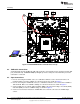
EVM Assembly Drawings and PCB Layout 8 www.ti.com EVM Assembly Drawings and PCB Layout The following figures (Figure 92 through Figure 101) show the design of the TPS59650EVM-753 printed circuit board. The EVM has been designed using 8 Layers circuit board with 1oz copper on outside layers. Figure 92. TPS59650EVM-753 Top Layer Assembly Drawing (Top view) Figure 93.
EVM Assembly Drawings and PCB Layout www.ti.com Figure 94. TPS59650EVM-753 Top Copper Figure 95.
EVM Assembly Drawings and PCB Layout www.ti.com Figure 96. TPS59650EVM-753 Internal Layer 2 Figure 97.
EVM Assembly Drawings and PCB Layout www.ti.com Figure 98. TPS59650EVM-753 Internal Layer 4 Figure 99.
EVM Assembly Drawings and PCB Layout www.ti.com Figure 100. TPS59650EVM-753 Internal Layer 6 Figure 101.
Bill of Materials www.ti.com 9 Bill of Materials The EVM major components list according to the schematic shown in the following pages. Table 13. EVM Major Components List QTY REF DES Description MFR Part Number 11 C1, C12, C31, C69, C74, C124, C159, C121, C130, C184, C204 Capacitor, Ceramic, 1nF, 50V, X7R, 10%, 0603 STD STD 5 C104, C108, C112, C115, C118 Capacitor, Ceramic, 33nF, 25V, X7R, 10%, 0603 STD STD 29 C128, C201, C192, C209, C218, C222, C226, C230 Capacitor, Ceramic, 0.
Bill of Materials www.ti.com Table 13. EVM Major Components List (continued) QTY REF DES Description MFR Part Number 5 D4, D5, D7, D8, D11 Diode, LED, Red Clear, 20mcd, 0.079x0.049 Lite On LTST-C170CKT 1 D6 Diode, Schottky, 200mA, 30V, SOT-23, Vishay-Liteon BAT54-V-GS08 1 FB1 Bead, SMD,Ferrite, 100MHz Max, 200mA, +/-25%, 0603 WE 74279266A 5 L1, L2, L3, L4, L5 Inductor, SMT, 0.36uH, 35A , 0.82mohm, 10x11.5mm Toko FCUL1040-H-R36M 1 L6 Inductor, SMT, 0.42uH, 17A , 1.5mohm, 8.7x7.
Bill of Materials www.ti.com Table 13. EVM Major Components List (continued) QTY REF DES Description MFR Part Number 20 R43, R49, R51, R60, R65, R71, R75, R85, R87, R93, R200, R201, R208, R209, R243, R249, R253, R254, R263, R265 Resistor, Chip, 0, 1/16W, 1%, 0402 STD STD 1 R21 Resistor, Chip, 200k, 1/10W, 1%, 0603 STD STD 2 R210, R211 Resistor, Chip, 3.
Schematics www.ti.com Table 13. EVM Major Components List (continued) QTY REF DES Description MFR Part Number 1 U9 IC, Quadruple 2-input positive –AND gates, SO-14 TI SN74HC08D 2 U10, U11 IC, Dual 4A High speed low side power MOSFET drivers, SO-8 TI UCC27324D 1 X1 Crystal, controlled oscillators, 0.150”x0.528” ABRACON ABLS-20.000MHZ-B2-T 1 Y1 Crystal, controlled oscillators, 0.150”x0.528” ABRACON ABLS-12.
6 1 R3 R4 54.9 TP18 R21 200k TP16 C17 0.33uF TP9 3 See Sheet 5 for FREQ selection R16 20.0k 1 R13 C22 1uF 5 See Sheet 5 for OCP selection and OSR setting R2 130 0 R24 C26 100pF 4.02k R23 TP21 C13 100pF 8.25k R6 TP3 1 C25 RT2 100k 15.4k R22 TP20 2 TP5 R26 100k 1 R25 1 C14 R18 10.0k TP8 15.4k R7 7 2.21 R14 2.21 R11 10 R5 TP17 C7 2.
22uF C51 22uF 22uF 22uF C52 C38 C37 TP29 TP26 22uF C53 22uF 22uF C54 1uF 2.21 C39 C33 R29 22uF C40 1 C36 22uF 22uF C56 Not used 22uF C55 C41 2.2uF 22uF C42 R28 2.21 10uF R31 0 10uF 22uF C58 C43 TP28 C57 TP25 TP24 TP23 10uF 10uF C59 C44 C27 10uF 10uF 22uF C60 C45 C28 10uF 1 C47 C31 1nF 10uF C62 1 C35 1 1 C48 0.
C94 22uF C93 22uF 1 1 22uF C95 1 C85 TP42 TP44 C84 TP34 C65 10uF TP37 C83 TP38 TP32 TP31 1 C96 2.21 R32 C66 10uF 1 1 22uF 22uF 1 C88 C82 2.2uF C79 2.2uF C69 1nF C87 C98 1uF C86 C80 R37 C75 1uF C68 10uF 2.21 C97 C67 10uF 1 C99 22uF C89 TP43 R34 2.21 22uF 22uF 22uF 22uF C101 C91 0 R41 0 R36 22uF C102 C72 10uF C90 TP45 2.21 R39 TP39 C71 10uF C100 TP36 C70 10uF 22uF C92 C73 10uF GND_PWR C74 1nF 1 0.36uH L4 Not used 1 C81 1 0.
R91 162k 17.8k R86 R79 162k 17.8k R74 R68 162k 17.8k R64 R56 162k 17.8k R50 R46 162k 17.8k R42 R92 28.7k RT7 100k R84 28.7k RT6 100k R70 28.7k RT5 100k R59 28.7k RT4 100k R48 28.
13 10 1 1 R129 R128 R96 R98 R100 R102 R105 R107 R109 R111 R113 R115 R117 R119 R121 R123 R125 R127 150k 100k 75.0k 56.2k 39.2k 30.1k 24.3k 20.0k 150k 100k 75.0k 56.2k 39.2k 30.1k 24.3k 20.0k 13 12 11 10 1 11 TP58 TP57 R120 R122 R124 R126 30.1k 24.3k 20.0k R112 150k R118 R110 20.0k 39.2k R108 24.3k 56.2k R106 30.1k R116 R103 39.2k R114 R101 56.2k 75.0k R99 100k R97 75.
14 TP62 To processor Q6 BSS123 D1 GREEN R130 180 R146 10 10 R143 R139 10.5k 1 R137 R132 10.0k 15 14 1 0 TP65 TP61 C127 0.1uF C131 10nF 15 J16 R135 2.21 0 R142 TP63 To controller R141 30.1k R134 1.00k C121 1nF S1: VCCIO Enable Pin 1 1 C156 1 TP60 TP59 1 C137 1 C158 22uF C148 TP68 R136 2.21 C157 22uF 22uF C155 22uF C147 C136 C135 2.2uF TP64 C146 C128 0.1uF VCCIO Output Selection: 1. Jumper shorts on pin1 and pin2 of J14 to set VCCIO: 1.05V(Default) 2.
Q9 BSS123 C165 10uF 0 R161 0 R148 10.0k C166 2.2uF R159 TP72 D3 GREEN R147 180 C171 0.22uF J20 C172 0.1uF TP79 R160 20.0k R158 10.0k R151 1.00k 1nF C184 R152 22.1k 0 R157 R149 10.0k C174 C162 10uF C175 C161 10uF 1 C169 1 1 10uF 10uF VDDQ Power 1 1 1 TP76 TP77 C183 L7 1.0uH C177 C159 1nF TP75 R155 C176 C163 10uF 10uF C179 10uF C180 10uF C181 10uF C182 S3/S5 Enable Control, See datasheet for detail 1 C160 10uF C173 0 R156 16 C178 TP78 2.
C197 0.01uF R184 100k R182 8.06k C198 0.1uF 0.1uF C201 R183 10.0k D6 BAT54 1 1 J23 1 17 R171 TP84 TP82 R185 10.0k 18 C199 0.1uF 10.0k R176 R170 TP86 R169 1 + C186 Silk: VCCIO_DL GFX_DL CPU_DL1 CPU_DL2 5V Bias Voltage Input TP87 1 + C187 VBAT Conversion Voltage Input: 9V -20V 18 U9:D U9:C U9:B SN74HC08D U9:A C202 1uF U11 UCC27324D C196 1uF U10 UCC27324D J23: Default setting: Jumper shorts on to Enable on board dynamic load 330 R186 0.
1 20 1 R191 C204 1nF R192 100 19 Q16 BSS123 D9 GREEN VR_ON 180 R215 BSS123 Q17 D10 GREEN TP98 C_PGOOD R216 180 10.0k R220 10pF C205 10pF C206 C203 0.1uF BSS123 Q18 D12 GREEN G_PGOOD TP97 10.0k R221 R222 180 D11 RED VR_HOT BSS83P Q15 Default Trim: R117 = Not used, R116 = 1.00k R219 10.0k R214 10.0k S4: IMVP-7 VR Enable: 1. Switch to "ON" position to Enable TPS59650 controller 2. Switch to "OFF" position to Disable TPS59650 controller(Default) Not used R210 3.
1 R223 R224 75.0 R225 130 R226 43.
uC Socket Others
V+ DM DP NC V- 22 J35 J34 GREEN D13 21 R234 470 FB1 J33 R229 R228 Jumper to use 5V from USB 33.2 33.2 R235 2.21k 22pF 10.0k R231 C214 22pF R227 C213 TP99 TP100 C209 0.1uF 22 21 1 1.50k 1 TP102 TP101 10.0k R230 1 C211 Y1 2 0 R233 0 R232 0.01uF C215 1 C212 For Internal software developmenet USB to DSP 5V Bias option: 1. Jumper shorts on J33, 5V Bias used from USB. If USB 5V is used, external 5V supply from J22 should not be used. 2.
4 TP108 3 U20:B U20:A R241 2.74k TP107 C218 0.1uF C217 0.1uF 6 C219 2 5 C220 C221 0.
26 1 0 1 TP111 C235 C236 R253 0 1.8nF C245 R252 2.00k C244 100pF R259 20.0k C237 22uF C243 5.62k 22uF 680pF R245 22uF C238 C239 10nF R258 3.09k 2200pF C247 1uF C242 22uF VIN 17 1 R256 SS IMON MODE VOUT EN FSET VFB COMP 1 TPS51318 U21 VBST VCCA GND PGOOD J42, J43: Optional VCCIO and VDDQ Enable 1. Jumper shorts on J42, J43 to Enable Optional VCCIO and VDDQ 2.
EVALUATION BOARD/KIT/MODULE (EVM) ADDITIONAL TERMS Texas Instruments (TI) provides the enclosed Evaluation Board/Kit/Module (EVM) under the following conditions: The user assumes all responsibility and liability for proper and safe handling of the goods. Further, the user indemnifies TI from all claims arising from the handling or use of the goods.
FCC Interference Statement for Class B EVM devices This equipment has been tested and found to comply with the limits for a Class B digital device, pursuant to part 15 of the FCC Rules. These limits are designed to provide reasonable protection against harmful interference in a residential installation. This equipment generates, uses and can radiate radio frequency energy and, if not installed and used in accordance with the instructions, may cause harmful interference to radio communications.
【Important Notice for Users of this Product in Japan】 】 This development kit is NOT certified as Confirming to Technical Regulations of Radio Law of Japan If you use this product in Japan, you are required by Radio Law of Japan to follow the instructions below with respect to this product: 1. 2. 3. Use this product in a shielded room or any other test facility as defined in the notification #173 issued by Ministry of Internal Affairs and Communications on March 28, 2006, based on Sub-section 1.
EVALUATION BOARD/KIT/MODULE (EVM) WARNINGS, RESTRICTIONS AND DISCLAIMERS For Feasibility Evaluation Only, in Laboratory/Development Environments. Unless otherwise indicated, this EVM is not a finished electrical equipment and not intended for consumer use.
IMPORTANT NOTICE Texas Instruments Incorporated and its subsidiaries (TI) reserve the right to make corrections, enhancements, improvements and other changes to its semiconductor products and services per JESD46, latest issue, and to discontinue any product or service per JESD48, latest issue. Buyers should obtain the latest relevant information before placing orders and should verify that such information is current and complete.