
Datasheet

SLVS216B − JUNE 1999 − JUNE 2008
1
POST OFFICE BOX 655303 • DALLAS, TEXAS 75265
features
D Up to 150-mA Output Current
D Less Than 10-mV
pp
Output Voltage Ripple
D No Inductors Required/Low EMI
D Regulated 5-V ±4% Output
D Only Four External Components Required
D Up to 90% Efficiency
D 2.7-V to 5.4-V Input Voltage Range
D 60-µA Quiescent Supply Current
D 0.05-µA Shutdown Current
D Load Isolated in Shutdown
D Space-Saving Thermally-Enhanced TSSOP
PowerPAD Package
D Evaluation Module Available
(TPS60110EVM−132)
applications
Replaces DC/DC Converters With Inductors in
− Battery-Powered Applications
− Li-Ion Battery to 5-V Conversion
− Portable Instruments
− Battery-Powered Microprocessor
Systems
− Miniature Equipment
− Backup-Battery Boost Converters
− PDAs
− Laptops
− Handheld Instrumentation
− Medical Instruments
description
The TPS60111 step-up, regulated charge pump
generates a 5-V ±4% output voltage from a 2.7-V
to 5.4-V input voltage (three alkaline, NiCd, or
NiMH batteries; or, one lithium or lithium ion
battery). Output current is 150 mA from a 3-V
input. Only four external capacitors are needed to
build a complete low-noise dc/dc converter. The
push-pull operating mode of two single-ended
charge pumps assures the low output voltage
ripple as current is continuously transferred to the
output. From a 3-V input, the TPS60111 can start
into full load with loads as low as 33 Ω.
The TPS60111 features either constant frequency
mode to minimize noise and output voltage ripple
or the power-saving pulse-skip mode to extend
battery life at light loads. The TPS60111 switching
frequency is 300 kHz. The logic shutdown function
reduces the supply current to 1-µA (max) and
disconnects the load from the input. Special
current-control circuitry prevents excessive cur-
rent from being drawn from the battery during
start-up. This dc/dc converter requires no
inductors and has low EMI. It is available in the
small 20-pin TSSOP PowerPAD package
(PWP).
Copyright 1999 − 2008, Texas Instruments Incorporated
! " #$%! " &$'(#! )!%*
)$#!" # ! "&%##!" &% !+% !%" %," "!$%!"
"!)) -!.* )$#! &#%""/ )%" ! %#%""(. #($)%
!%"!/ (( &%!%"*
Please be aware that an important notice concerning availability, standard warranty, and use in critical applications of
Texas Instruments semiconductor products and disclaimers thereto appears at the end of this data sheet.
PowerPAD is a trademark of Texas Instruments Incorporated.
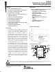
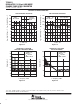
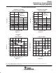
output voltage ripple
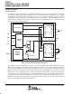
typical operating circuit
Figure 1
SKIP =COM = CLK = 0 V
V
IN
= 3.6 V
I
O
= 150 mA
C
O
= 22 µF + 10 µF
X5R Ceramic
5.2
5
5.05
5.1
5.15
4.8
4.85
4.9
4.95
− Output Voltage − VV
O
52.50 0.5 1 1.5 2 3 3.5 4 4.5
t − Time − µs
IN
IN
C1+
C1−
ENABLE
OUT
OUT
FB
C2+
C2−
SYNC
SKIP COM CLK
PGND GND
INPUT
2.7 V to
5.4 V
C
IN
4.7 µF
OUTPUT
5 V
150 mA
C
O
15 µF
C
2F
1 µF
C
1F
1 µF
+
OFF/ON
TPS60110
+