TPS60300, TPS60301, TPS60302, TPS60303 SINGLE-CELL TO 3.0-V/3.3-V, 20-mA DUAL OUTPUT, HIGH-EFFICIENCY CHARGE PUMP SLVS302A – DECEMBER 2000 – REVISED MARCH 2001 features applications D Regulated 3-V or 3.3-V Output Voltage With D D D D D D D D D D D D D up to 20-mA Output Current From a 0.9-V to 1.8-V Input Voltage Range High Power Conversion Efficiency (up to 90%) Over a Wide Output Current Range, Optimized for 1.
TPS60300, TPS60301, TPS60302, TPS60303 SINGLE-CELL TO 3.0-V/3.3-V, 20-mA DUAL OUTPUT, HIGH-EFFICIENCY CHARGE PUMP SLVS302A – DECEMBER 2000 – REVISED MARCH 2001 description (continued) Output 1 (OUT1) can deliver a maximum of 40 mA, from a 1-V input, with output 2 (OUT2) not loaded. OUT2 can deliver a maximum of 20 mA, from a 1-V input, with OUT1 not loaded. Both outputs can be loaded in the same time, but the total output current of the first voltage doubler must not exceed 40 mA.
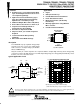
TPS60300, TPS60301, TPS60302, TPS60303 SINGLE-CELL TO 3.0-V/3.3-V, 20-mA DUAL OUTPUT, HIGH-EFFICIENCY CHARGE PUMP SLVS302A – DECEMBER 2000 – REVISED MARCH 2001 TPS60300 and TPS60301 functional block diagram C1F C1– C1+ CP1 2x (Doubler) Charge Pump VIN OUT1 _ Oscillator Control EN + PG (Push-Pull Output for TPS60302 and TPS60303) _ Reg + Vref CP2 1.5x/2x Charge Pump C2– + _ OUT2 C2+ GND C2F Terminal Functions TERMINAL NAME NO.
TPS60300, TPS60301, TPS60302, TPS60303 SINGLE-CELL TO 3.0-V/3.3-V, 20-mA DUAL OUTPUT, HIGH-EFFICIENCY CHARGE PUMP SLVS302A – DECEMBER 2000 – REVISED MARCH 2001 detailed description operating principle The TPS6030x charge pumps are voltage quadruplers that provide a regulated 3.3-V or 3.0-V output from a 0.9-V to 1.8-V input. They deliver a maximum load current of 20 mA.
TPS60300, TPS60301, TPS60302, TPS60303 SINGLE-CELL TO 3.0-V/3.3-V, 20-mA DUAL OUTPUT, HIGH-EFFICIENCY CHARGE PUMP SLVS302A – DECEMBER 2000 – REVISED MARCH 2001 absolute maximum ratings over operating free-air temperature (unless otherwise noted)† Input voltage, VI (IN to GND) (see Note 1) . . . . . . . . . . . . . . . . . . . . . . . . . . . . . . . . . . . . . . . . . . . . . –0.3 V to 2 V Output voltage, VO (OUT1,OUT2, EN, PG to GND) (see Note 1) . . . . . . . . . . . . . . . . . . . . . . . . –0.
TPS60300, TPS60301, TPS60302, TPS60303 SINGLE-CELL TO 3.0-V/3.3-V, 20-mA DUAL OUTPUT, HIGH-EFFICIENCY CHARGE PUMP SLVS302A – DECEMBER 2000 – REVISED MARCH 2001 electrical characteristics at CIN = C1F = C2F = C(OUT1) = C(OUT2) = 1 µF, TC = –40°C to 85°C, VIN = 1.
TPS60300, TPS60301, TPS60302, TPS60303 SINGLE-CELL TO 3.0-V/3.3-V, 20-mA DUAL OUTPUT, HIGH-EFFICIENCY CHARGE PUMP SLVS302A – DECEMBER 2000 – REVISED MARCH 2001 electrical characteristics at CIN = C1F = C2F = C(OUT1) = C(OUT2) = 1 µF, TC = –40°C to 85°C, VIN = 1.0 V, V(EN) = VIN (unless otherwise noted) (continued) PARAMETER TEST CONDITIONS Output load regulation VIN = 1.25 V, TC = 25°C 2 mA < IO(OUT2) < 20 mA Output line regulation 1.0 V < VIN < 1.
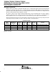
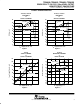
TPS60300, TPS60301, TPS60302, TPS60303 SINGLE-CELL TO 3.0-V/3.3-V, 20-mA DUAL OUTPUT, HIGH-EFFICIENCY CHARGE PUMP SLVS302A – DECEMBER 2000 – REVISED MARCH 2001 TYPICAL CHARACTERISTICS Table of Graphs FIGURE η Efficiency vs Output current 1, 2 IS IQ Supply current vs Output current 3 Quiescent current vs Input voltage 4 VO(OUT2) VO(OUT1) Output voltage at OUT2 vs Output current Output voltage at OUT1 vs Output current at 25°C, VIN = 0.9 V, 1.1 V, 1.25 V, 1.4 V, 1.6 V, 1.
TPS60300, TPS60301, TPS60302, TPS60303 SINGLE-CELL TO 3.0-V/3.3-V, 20-mA DUAL OUTPUT, HIGH-EFFICIENCY CHARGE PUMP SLVS302A – DECEMBER 2000 – REVISED MARCH 2001 TYPICAL CHARACTERISTICS TPS60300, TPS60302 TPS60301, TPS60303 EFFICIENCY vs OUTPUT CURRENT EFFICIENCY vs OUTPUT CURRENT 90 90 VI = 0.9 V 80 VI = 0.9 V 80 70 70 VI = 1.25 V VI = 1.25 V 60 50 Efficiency – % Efficiency – % 60 VI = 1.8 V 40 50 40 30 30 20 20 10 10 0 0.1 1 10 IO – Output Current – mA VI = 1.8 V 0 0.
TPS60300, TPS60301, TPS60302, TPS60303 SINGLE-CELL TO 3.0-V/3.3-V, 20-mA DUAL OUTPUT, HIGH-EFFICIENCY CHARGE PUMP SLVS302A – DECEMBER 2000 – REVISED MARCH 2001 TYPICAL CHARACTERISTICS TPS60300, TPS60302 TPS60301, TPS60303 OUTPUT VOLTAGE (OUT2) vs OUTPUT CURRENT (OUT2) OUTPUT VOLTAGE (OUT2) vs OUTPUT CURRENT (OUT2) 3.4 3.2 VI = 1.8 V VO – Output Voltage (OUT2) – V VO – Output Voltage (OUT2) – V 3.1 3.2 VI = 1.25 V VI = 1.1 V 3 VI = 0.9 V 2.8 VI = 1.25 V VI = 1.8 V 3 VI = 1.1 V 2.9 VI = 0.
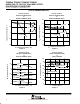
TPS60300, TPS60301, TPS60302, TPS60303 SINGLE-CELL TO 3.0-V/3.3-V, 20-mA DUAL OUTPUT, HIGH-EFFICIENCY CHARGE PUMP SLVS302A – DECEMBER 2000 – REVISED MARCH 2001 TYPICAL CHARACTERISTICS TPS60300, TPS60302 TPS6030x OUTPUT VOLTAGE (OUT2) vs INPUT VOLTAGE OUTPUT VOLTAGE (OUT1) vs INPUT VOLTAGE 3.1 3.5 IO(OUT2) = 0.1 mA IO(OUT1) = 0.1 mA VO – Output Voltage (OUT1) – V VO – Output Voltage (OUT2) – V IO(OUT2) = 1 mA 3.05 3 IO(OUT2) = 10 mA IO(OUT2) = 20 mA 2.95 2.9 2.85 0.8 1 1.2 1.
TPS60300, TPS60301, TPS60302, TPS60303 SINGLE-CELL TO 3.0-V/3.3-V, 20-mA DUAL OUTPUT, HIGH-EFFICIENCY CHARGE PUMP SLVS302A – DECEMBER 2000 – REVISED MARCH 2001 TYPICAL CHARACTERISTICS TPS60300, TPS60302 MINIMUM INPUT VOLTAGE vs OUTPUT CURRENT TPS6030x OUTPUT VOLTAGE RIPPLE (OUT2) 1.20 IO(OUT2) = 20 mA, VI = 1.2 V VI(min)– Minimum Input Voltage – V 1.15 10 mV/DIV 1.10 TA = 85°C 1.05 TA = –40°C 1.00 0.95 0.90 0.85 TA = 25°C 0.80 0.75 500 ns/DIV 0.70 0.
TPS60300, TPS60301, TPS60302, TPS60303 SINGLE-CELL TO 3.0-V/3.3-V, 20-mA DUAL OUTPUT, HIGH-EFFICIENCY CHARGE PUMP SLVS302A – DECEMBER 2000 – REVISED MARCH 2001 TYPICAL CHARACTERISTICS SWITCHING FREQUENCY vs INPUT VOLTAGE LOAD TRANSIENT RESPONSE 730 20 mV/DIV Switching Frequency – kHz 720 TA = 85°C 710 VO(OUT2) 700 VI = 1.25 V, Load Step 2 mA to 18 mA to 2 mA, TA = 25°C TA = 25°C 690 TA = –40°C 680 670 10 mA/DIV 660 20 µs/DIV 650 0.8 1.3 VI – Input Voltage – V IO(OUT2) 1.
TPS60300, TPS60301, TPS60302, TPS60303 SINGLE-CELL TO 3.0-V/3.3-V, 20-mA DUAL OUTPUT, HIGH-EFFICIENCY CHARGE PUMP SLVS302A – DECEMBER 2000 – REVISED MARCH 2001 APPLICATION INFORMATION design procedure capacitor selection The TPS6030x devices require only five external capacitors. Their values are closely linked to the required output current and the output noise and ripple requirements. It is possible to only use 1-µF capacitors of the same type.
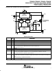
TPS60300, TPS60301, TPS60302, TPS60303 SINGLE-CELL TO 3.0-V/3.3-V, 20-mA DUAL OUTPUT, HIGH-EFFICIENCY CHARGE PUMP SLVS302A – DECEMBER 2000 – REVISED MARCH 2001 APPLICATION INFORMATION INPUT 0.9 V to 1.8 V 3 + CIN 1 µF + R1 TPS60300 4 C1F 1 µF 2 10 PG C1+ C2– EN OUT1 8 C2F 1 µF 5 + GND OFF/ON C(OUT2) 1 µF PG 7 C2+ C1– 1 OUTPUT 3.3 V, 20 mA 6 OUT2 VIN 9 C(OUT1) 1 µF Figure 20.
TPS60300, TPS60301, TPS60302, TPS60303 SINGLE-CELL TO 3.0-V/3.3-V, 20-mA DUAL OUTPUT, HIGH-EFFICIENCY CHARGE PUMP SLVS302A – DECEMBER 2000 – REVISED MARCH 2001 design procedure (continued) Due to R(PG,1), an output filter can easily be formed with an output capacitor (CPG). Cut-off frequency is given by: 1 ƒc + (1) 2pR C (PG,1) (PG) and ratio VOUT/VIN is: Ť V V (PG,1) O(OUT2) Ť + 1 Ǹ ǒ 1 ) 2pƒ R C (PG,1) (PG) Ǔ (2) 2 with R(PG,1) = 15 Ω, C(PG) = 0.
TPS60300, TPS60301, TPS60302, TPS60303 SINGLE-CELL TO 3.0-V/3.3-V, 20-mA DUAL OUTPUT, HIGH-EFFICIENCY CHARGE PUMP SLVS302A – DECEMBER 2000 – REVISED MARCH 2001 design procedure (continued) 3 CIN 1 µF ON TPS60302 4 1.5 V C1F 1 µF OUT2 VIN + 2 1 PG C1+ C2+ C1– C2– EN OUT1 6 MSP430 C(OUT2) 1 µF 10 7 C2F 1 µF 8 CPG 0.1 µF Amplifier Sensor 5 + GND R1 1 MΩ Display + 9 C(OUT1) 1 µF Figure 23.
TPS60300, TPS60301, TPS60302, TPS60303 SINGLE-CELL TO 3.0-V/3.3-V, 20-mA DUAL OUTPUT, HIGH-EFFICIENCY CHARGE PUMP SLVS302A – DECEMBER 2000 – REVISED MARCH 2001 layout and board space (continued) PG 9,8 mm OUT2 GND GND VIN OUT1 0 mm EN 0 mm 7,62 mm Figure 24. Recommended PCB Layout for TPS6030x (top layer) device family products Other charge pump dc-dc converters in this family are: Table 5. Product Identification PART NUMBER DESCRIPTION TPS60100 2-cell to regulated 3.
TPS60300, TPS60301, TPS60302, TPS60303 SINGLE-CELL TO 3.0-V/3.3-V, 20-mA DUAL OUTPUT, HIGH-EFFICIENCY CHARGE PUMP SLVS302A – DECEMBER 2000 – REVISED MARCH 2001 MECHANICAL DATA DGS (S-PDSO-G10) PLASTIC SMALL-OUTLINE PACKAGE 0,27 0,17 0,50 10 0,25 M 6 0,15 NOM 3,05 2,95 4,98 4,78 Gage Plane 0,25 1 0°–ā6° 5 3,05 2,95 0,69 0,41 Seating Plane 1,07 MAX 0,15 0,05 0,10 4073272/A 03/98 NOTES: A. All linear dimensions are in millimeters. B. This drawing is subject to change without notice. C.
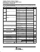
PACKAGE OPTION ADDENDUM www.ti.
PACKAGE OPTION ADDENDUM www.ti.com 5-Oct-2007 (3) MSL, Peak Temp. -- The Moisture Sensitivity Level rating according to the JEDEC industry standard classifications, and peak solder temperature. Important Information and Disclaimer:The information provided on this page represents TI's knowledge and belief as of the date that it is provided. TI bases its knowledge and belief on information provided by third parties, and makes no representation or warranty as to the accuracy of such information.
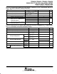
PACKAGE MATERIALS INFORMATION www.ti.com 29-Jul-2008 TAPE AND REEL INFORMATION *All dimensions are nominal Device Package Package Pins Type Drawing SPQ Reel Reel Diameter Width (mm) W1 (mm) A0 (mm) B0 (mm) K0 (mm) P1 (mm) W Pin1 (mm) Quadrant TPS60300DGSR MSOP DGS 10 2500 330.0 12.4 5.3 3.4 1.4 8.0 12.0 Q1 TPS60301DGSR MSOP DGS 10 2500 330.0 12.4 5.3 3.4 1.4 8.0 12.0 Q1 TPS60302DGSR MSOP DGS 10 2500 330.0 12.4 5.3 3.4 1.4 8.0 12.
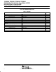
PACKAGE MATERIALS INFORMATION www.ti.com 29-Jul-2008 *All dimensions are nominal Device Package Type Package Drawing Pins SPQ Length (mm) Width (mm) Height (mm) TPS60300DGSR MSOP DGS 10 2500 340.5 338.1 20.6 TPS60301DGSR MSOP DGS 10 2500 340.5 338.1 20.6 TPS60302DGSR MSOP DGS 10 2500 346.0 346.0 29.0 TPS60303DGSR MSOP DGS 10 2500 340.5 338.1 20.
IMPORTANT NOTICE Texas Instruments Incorporated and its subsidiaries (TI) reserve the right to make corrections, modifications, enhancements, improvements, and other changes to its products and services at any time and to discontinue any product or service without notice. Customers should obtain the latest relevant information before placing orders and should verify that such information is current and complete.