
Datasheet


SLVS324A − JULY 2001 REVISED NOVEMBER 2004
1
WWW.TI.COM
features
D Inverts Input Supply Voltage
D Up to 60-mA Output Current
D Only Three Small 1-µF Ceramic Capacitors
Needed
D Input Voltage Range From 1.6 V to 5.5 V
D PowerSave-Mode for Improved Efficiency
at Low Output Currents (TPS60400)
D Device Quiescent Current Typical 65 µA
D Integrated Active Schottky-Diode for
Start-Up Into Load
D Small 5-Pin SOT23 Package
D Evaluation Module Available
TPS60400EVM−178
applications
D LCD Bias
D GaAs Bias for RF Power Amps
D Sensor Supply in Portable Instruments
D Bipolar Amplifier Supply
D Medical Instruments
D Battery-Operated Equipment
description
The TPS6040x is a family of devices that generate an unregulated negative output voltage from an input voltage
ranging from 1.6 V to 5.5 V. The devices are typically supplied by a preregulated supply rail of 5 V or 3.3 V. Due
to its wide input voltage range, two or three NiCd, NiMH, or alkaline battery cells, as well as one Li-Ion cell can
also power them.
Only three external 1-µF capacitors are required to build a complete dc/dc charge pump inverter. Assembled
in a 5-pin SOT23 package, the complete converter can be built on a 50 mm
2
board area. Additional board area
and component count reduction is achieved by replacing the Schottky diode that is typically needed for start-up
into load by integrated circuitry.
The TPS6040x can deliver a maximum output current of 60 mA with a typical conversion efficiency of greater
than 90% over a wide output current range. Three device options with 20-kHz, 50-kHz, and 250-kHz fixed
frequency operation are available. One device comes with a variable switching frequency to reduce operating
current in applications with a wide load range and enables the design with low-value capacitors.
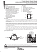
typical application circuit
TPS60400
C
FLY−
C
FLY+
35
OUTIN
GND
1
2
4
C
I
1 µF
C
O
1 µF
Output
−1.6 V to −5.5 V,
Max 60 mA
Input
1.6 V to 5.5 V
C
(fly)
1 µF
−5
−4
−3
−2
−1
0
012345
I
O
= 60 mA
I
O
= 30 mA
I
O
= 1 mA
T
A
= 25°C
V
I
− Input Voltage − V
− Output Voltage − V
TPS60400
OUTPUT VOLTAGE
vs
INPUT VOLTAGE
V
O
Copyright 2001−2004, Texas Instruments Incorporated
Please be aware that an important notice concerning availability, standard warranty, and use in critical applications of
Texas Instruments semiconductor products and disclaimers thereto appears at the end of this data sheet.
3
2
4
5
DBV PACKAGE
(TOP VIEW)
1
OUT
IN
C
FLY−
C
FLY+
GND
!" # $%&" !# '%()$!" *!"&+
*%$"# $ " #'&$$!"# '& ",& "&# &-!# #"%&"#
#"!*!* .!!"/+ *%$" '$&##0 *&# " &$&##!)/ $)%*&
"&#"0 !)) '!!&"&#+