
Datasheet
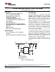
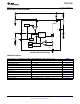

VIN5V
L1
10 Hm
D1
VIN SW
FB
GND
CTRL
COMP
C2
4.7 Fm
C3
10nF
TPS 61170
R1
87.6kW
VOUT 12V/300mA
R2
10kW
R3
4.99kW
C1
4.7 Fm
L1: TOKO#A915_Y-100M
C1:MurataGRM188R61A475K
C2:MurataGRM21BR61E475K
D1:
ONsemiMBR0540T1
*R3,C3:CompensationRCnetwork
TPS61170-Q1
www.ti.com
SLVSAX2 – SEPTEMBER 2011
1.2A High Voltage Boost Converter in 2x2mm
2
QFN Package
Check for Samples: TPS61170-Q1
1
FEATURES
DESCRIPTION
• Qualified for Automotive Applications
The TPS61170-Q1 is a monolithic, high-voltage
• 3-V to 18-V Input Voltage Range
switching regulator with integrated 1.2-A, 40-V power
• High Output Voltage: Up to 38 V
MOSFET. It can be configured in several standard
switching-regulator topologies, including boost and
• 1.2-A integrated Switch
SEPIC. The device has a wide input-voltage range to
• 1.2-MHz Fixed Switching Frequency
support applications with input voltage from multi-cell
• 12 V at 300 mA and 24 V at 150 mA from 5-V
batteries or regulated 5-V, 12-V power rails.
Input (Typical)
The TPS61170-Q1 operates at a 1.2-MHz switching
• Up to 93% Efficiency
frequency, allowing the use of low-profile inductors
• On-The-Fly Output Voltage Reprogramming
and low-value ceramic input and output capacitors.
External loop compensation components give the
• Skip-Switching Cycle for Output Regulation at
user flexibility to optimize loop compensation and
Light Load
transient response. The device has built-in protection
• Built-in Soft Start
features, such as pulse-by-pulse overcurrent limit,
• 6-Pin, 2 mm × 2 mm QFN Package
soft start and thermal shutdown.
The reference voltage to which the FB pin regulates
APPLICATIONS
is 1.229V. The reference voltage can be lowered
• 5-V to 12-V and 24-V, 12-V to 24-V Boost using a 1-wire digital interface (Easyscale™ protocol)
through the CTRL pin. Alternatively, a pulse
Converter
width-modulation (PWM) signal can be applied to the
• Buck Boost Regulation Using SEPIC Topology
CTRL pin. The duty cycle of the signal reduces the
feedback reference voltage proportionally.
The TPS61170-Q1 is available in a 6-pin 2 mm × 2
mm QFN package, allowing a compact power-supply
solution.
Figure 1. Typical Application
1
Please be aware that an important notice concerning availability, standard warranty, and use in critical applications of Texas
Instruments semiconductor products and disclaimers thereto appears at the end of this data sheet.
PRODUCTION DATA information is current as of publication date.
Copyright © 2011, Texas Instruments Incorporated
Products conform to specifications per the terms of the Texas
Instruments standard warranty. Production processing does not
necessarily include testing of all parameters.