
Datasheet
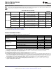
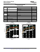

0
10
20
30
40
50
60
70
80
90
100
Efficiency - %
.
I - Output Current - mA
O
V - Input Voltage - V
I
2
.
7
3.0
3.3
3.6
3.9
4.2
4.5
4.8
5.1
5.4
0.1
0.2
0.4
0.8
1.6
3.2
6.2
12.6
25.1
50.1
100.1
199.6
398.1
794.3
.
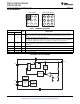
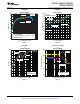
V = 5.0 V
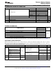
O
C
4.7
I
μF
C
10 uF
O
SW
VIN
EN
VOUT
BP
GND
L
1 μH
V
IN
2.65 V .. 4.85 V
V
OUT
5.0 V @ 700mA
TPS61256
TPS61253, TPS61254, TPS61256
TPS61258, TPS61259
www.ti.com
SLVSAG8C –SEPTEMBER 2011–REVISED AUGUST 2012
3.5-MHz HIGH EFFICIENCY STEP-UP CONVERTER IN CHIP SCALE PACKAGING
Check for Samples: TPS61253, TPS61254, TPS61256, TPS61258, TPS61259
1
FEATURES
DESCRIPTION
• 93% Efficiency at 3.5MHz Operation
The TPS6125x device provides a power supply
• 22µA Quiescent Current in Standby Mode
solution for battery-powered portable applications.
Intended for low-power applications, the TPS6125x
• 36µA Quiescent Current in Normal Operation
supports up to 800-mA load current from a battery
• Wide V
IN
Range From 2.3V to 5.5V
discharged as low as 2.65V and allows the use of low
• V
IN
≥ V
OUT
Operation
cost chip inductor and capacitors.
• I
OUT
≥800mA at V
OUT
= 4.5V, V
IN
≥2.65V
With a wide input voltage range of 2.3V to 5.5V, the
• I
OUT
≥1000mA at V
OUT
= 5.0V, V
IN
≥3.3V
device supports applications powered by Li-Ion
batteries with extended voltage range. Different fixed
• I
OUT
≥1500mA (Peak) at V
OUT
= 5.0V, V
IN
≥3.3V
voltage output versions are available from 3.15V to
• ±2% Total DC Voltage Accuracy
5.0V.
• Light-Load PFM Mode
The TPS6125x operates at a regulated 3.5-MHz
• Selectable Standby Mode or True Load
switching frequency and enters power-save mode
Disconnect During Shutdown
operation at light load currents to maintain high
• Thermal Shutdown and Overload Protection
efficiency over the entire load current range. The
PFM mode extends the battery life by reducing the
• Only Three Surface-Mount External
quiescent current to 36μA (typ) during light load
Components Required
operation.
• Total Solution Size <25mm
2
In addition, the TPS6125x device can also maintain
• 9-Pin NanoFree
TM
(CSP) Packaging
its output biased at the input voltage level. In this
mode, the synchronous rectifier is current limited
APPLICATIONS
allowing external load (e.g. audio amplifier) to be
• Cell Phones, Smart-Phones
powered with a restricted supply. In this mode, the
quiescent current is reduced to 22µA. Input current in
• Mono and Stereo APA Applications
shutdown mode is less than 1µA (typ), which
• USB Charging Port (5V)
maximizes battery life.
The TPS6125x offers a very small solution size due
spacer
to minimum amount of external components. It allows
spacer
the use of small inductors and input capacitors to
achieve a small solution size. During shutdown, the
load is completely disconnected from the battery.
Figure 2. Smallest Solution Size Application
Figure 1. Efficiency vs. Load Current
1
Please be aware that an important notice concerning availability, standard warranty, and use in critical applications of
Texas Instruments semiconductor products and disclaimers thereto appears at the end of this data sheet.
UNLESS OTHERWISE NOTED this document contains
Copyright © 2011–2012, Texas Instruments Incorporated
PRODUCTION DATA information current as of publication date.
Products conform to specifications per the terms of Texas
Instruments standard warranty. Production processing does not
necessarily include testing of all parameters.