
Datasheet
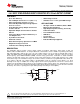
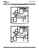

L
C
1
10µF
L
1
4.7
µ
H
VIN
VOUT
FB
C
2
10µF
EN
GND
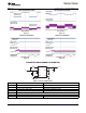
TPS61260
V
OUT
0.8 V t
o 4.0 V
V
IN
R
1
R
2
RI
R
3
TPS61260, TPS61261
www.ti.com
SLVSA99A –MAY 2011–REVISED FEBRUARY 2013
0.8-V INPUT SYNCHRONOUS BOOST CONVERTER WITH 100-mA OUTPUT CURRENT
1
FEATURES
• Up to 95% Efficiency • Undervoltage Lockout
• 100 mA Output Current at 3.3 V
out
(VIN > 1 V) • Available in a 2 × 2 mm, 6-pin SON Package
• Input Voltage Range from 0.8 V to 4.0 V
APPLICATIONS
• Fixed and Adjustable Output Voltage Options
• All single or dual cell Alkaline, NiCd or NiMH
from 1.8 V to 4.0 V
Battery Powered Products
• Programmable Average Output Current from
• High Output Impedance Battery (Coin Cells)
10 mA to 100 mA
Powered Products
• Adjustable Output Current Limit for Smallest
• Personal Medical Products
Inductor
• LED Driver
• Power Save Mode for Improved Efficiency at
Low Output Power
• Laser Pointer
• 29 µA Quiescent Current
• Wireless Headsets
• Advanced Softstart
• Industrial Metering Equipment
• Quasi Fixed Frequency Operation at 2.5 MHz
• Output Overvoltage Protection
• Load Disconnect During Shutdown
DESCRIPTION
The TPS6126x devices provide a power supply solution for products powered by either single or dual cell
alkaline, NiCd or NiMH batteries. Its unique advanced softstart makes it also suitable for products powered by
high output impedance battery types, like coin cells. Output currents can go as high as 100 mA while using a
single cell alkaline battery, and discharge it down to 0.8 V or lower. The boost converter is based on a quasi
fixed frequency, pulse-width-modulation (PWM) controller using synchronous rectification to obtain maximum
efficiency. At low load currents, the converter enters Power Save Mode to ensure high efficiency over a wide
load current range. The maximum average current in the switches is limited to a programmable value which can
go as high as 700 mA. The output voltage is programmable using an external resistor divider, or is fixed
internally on the chip. In addition, the average output current can be programmed as well. The converter then
regulates the programmed output voltage or the programmed output current, which ever demands lower output
power. The converter can be disabled to minimize battery drain. During shutdown, the load is disconnected from
the battery. The device is packaged in a 6-pin SON package measuring 2 × 2 mm (DRV).
1
Please be aware that an important notice concerning availability, standard warranty, and use in critical applications of
Texas Instruments semiconductor products and disclaimers thereto appears at the end of this data sheet.
PRODUCTION DATA information is current as of publication date.
Copyright © 2011–2013, Texas Instruments Incorporated
Products conform to specifications per the terms of the Texas
Instruments standard warranty. Production processing does not
necessarily include testing of all parameters.